Saturday, November 30, 2013
6 Watt Audio Amplifier Schematic Circuit with TDA1519
 6 Watt Audio Amplifier Schematic Circuit with TDA1519
The audio amplifier circuit is on the TDA1519 amplifier IC that is based in audio applications, which is not a aerial achievement ability can be used. The ambit TDA1519 is a ability of 2×6 watts.
The TDA1519 is an amplifier congenital Class B dual-output advance in a 9-by-line (SIL) artificial amalgamation boilerplate achievement is primarily developed for car radio applications.
Key Features of the audio amplifier IC TDA1519 are: Requires few alien components, anchored gain, acceptable bounce drive, aphasiac / standby mode, thermal protection, about-face polarity safe. Tda1519 amplifier ability rating, 14.4 volts.
Friday, November 29, 2013
NE555 IC Timer
The 555 Timer is an integrated circuit (chip) implementing a variety of timer and multivibrator applications. The IC was designed and invented by Hans R. Camenzind. It was designed in 1970 and introduced in 1971 by Signetics (later acquired by Philips). The original name was the SE555/NE555 and was called "The IC Time Machine".
 The 555 gets its name from the three 5-k Ohm resistors used in typical early implementations. It is still in wide use, thanks to its ease of use, low price and good stability. As of 2003[update], 1 billion units are manufactured every year.
The 555 timer is one of the most popular and versatile integrated circuits ever produced. It includes 23 transistors, 2 diodes and 16 resistors on a silicon chip installed in an 8-pin mini dual-in-line package (DIP-8).
The 555 has three operating modes:
* Monostable mode: in this mode, the 555 functions as a "one-shot". Applications include timers, missing pulse detection, bouncefree switches, touch switches, Frequency Divider,Capacitance Measurement, Pulse Width Modulation (PWM) etc
* Astable - Free Running mode: the 555 can operate as an oscillator. Uses include LED and lamp flashers, pulse generation, logic clocks, tone generation, security alarms, pulse position modulation, etc.
* Bistable mode or Schmitt trigger: the 555 can operate as a flip-flop, if the DIS pin is not connected and no capacitor is used. Uses include bouncefree latched switches, etc.
The connection of the pins is as follows:

Nr. Name Purpose
1 GND Ground, low level (0V)
2 TR A short pulse high → low on the trigger starts the timer
3 Q During a timing interval, the output stays at +VCC
4 R A timing interval can be interrupted by applying a reset pulse to low (0V)
5 CV Control voltage allows access to the internal voltage divider (2/3 VCC)
6 THR The threshold at which the interval ends (it ends if U.thr → 2/3 VCC)
7 DIS Connected to a capacitor whose discharge time will influence the timing interval
8 V+, VCC The positive supply voltage which must be between 3 and 15 V
In the astable mode, the high time from each pulse is given by
high = 0.693.(R1 + R2).C
and the low time from each pulse is given by
low = 0.693.R2.C
where R1 and R2 are the values of the resistors in ohms and C is the value of the capacitor in farads.
Specs
These specifications apply to the NE555. Other 555 timers can have better specifications depending on the grade (military, medical, etc).
* Supply voltage (VCC) 4.5 to 15 V
* Supply current (VCC = +5 V) 3 to 6 mA
* Supply current (VCC = +15 V) 10 to 15 mA
* Output current (maximum) 200 mA
* Power dissipation 600 mW
* Operating temperature 0 to 70 °C
Thursday, November 28, 2013
Simple 4 Channel Video Amplifier Using NJM2582
A very simple 4 channel video amplifier electronic circuit project can be designed using NJM2582 ic suitable for video applications with SCART connector . Models of the circuit is very simple and require few external electronic parts .
Simple 4 Channel Video Amplifier Circuit diagram

Some features of the NJM2582 are : Operating Voltage ±5V, +5V, +11V ; 6input 4output , 2input 1output Video SW , Internal LPF , 6dB Amplifier , Internal 75Ω Driver Circuit , DC output for SCART (FUNCTION SW, BLANKING) .
Simple 4 Channel Video Amplifier Circuit diagram
Wednesday, November 27, 2013
Volt meters ampere meter with PIC
Volt meters & ampere meter with PIC can be used to measure voltage and current simultaneously. The series of volt meters & ampere meter with PIC16F876A PIC is used as a data processor voltage and current are measured.
This circuit uses the viewer in the form of 16 × 2 LCD used for the data menmpilkan voltage and current measurements. In the article volt meter and ampere meter with PIC are discussed kerannya limited to devices only. More detail can be seen from the image sequence volt meter and ampere meter with PIC below.
The images of Volt Meter & Ampere Meter With PIC Circuit
 |
| Volt meters & ampere meter with PIC |
Tuesday, November 26, 2013
Simple Water Activated Alarm
The circuit uses a 555 timer wired as an astable oscillator and powered by the emitter current of the BC109C. Under dry conditions, the transistor will have no bias current and be fully off. As the probes get wet, a small current flows between base and emitter and the transistor switches on. A larger current flows in the collector circuit enabling the 555 osillator to sound.
Simple Water Activated Alarm Circuit diagram :

An On/Off switch is provided and remember to use a non-reactive metal for the probe contacts. Gold or silver plated contacts from an old relay may be used, however a cheap alternative is to wire alternate copper strips from a piece of veroboard. These will eventually oxidize over but as very little current is flowing in the base circuit, the higher impedance caused by oxidization is not important. No base resistor is necessary as the transistor is in emitter follower, current limit being the impedance at the emitter (the oscillator circuit).
Simple Water Activated Alarm Circuit diagram :
An On/Off switch is provided and remember to use a non-reactive metal for the probe contacts. Gold or silver plated contacts from an old relay may be used, however a cheap alternative is to wire alternate copper strips from a piece of veroboard. These will eventually oxidize over but as very little current is flowing in the base circuit, the higher impedance caused by oxidization is not important. No base resistor is necessary as the transistor is in emitter follower, current limit being the impedance at the emitter (the oscillator circuit).
Monday, November 25, 2013
Basically the DAC circuit
Basically the DAC circuit is made to meet the need for the level of influence in the development of digital electronic circuits electronics world.
Since the discovery of Silicon and Germanium semiconductor material then quickly there was a revolution in terms of simplicity and accuracy of an electronic circuit. Besides, with the implementation of digital circuits will support at all in terms of data storage and mobility. Lots of data can now be operated with a computer is a data converted from analog signals. For example a voice signal or analog form of video can be played and stored using a computer after analog signals are converted into digital data.
 Advantages possessed by the digital data than analog signal is a certainty the nature of the data or logic. Digital data only can be divided into two kinds of logic high "1" and logic low "0". Logic 1 represents 5 volts and low logic voltage 0 volts represents. Examples of the advantages of digital signals over analog signals is on television or digital radio receiver. By implementing a digital system signals emitted by television or radio stations will form the data 1 and 0, so at the time of the transmission or delivery of data signals that change or damaged by the interruption of transmission will hardly change the logic of the signals. But if the transmitted signal is the original signal in the form of an analog signal then if just a little damage due to interruption of transmission, the signal to be received is a signal that has been damaged serve targeted.
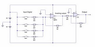
In the DAC circuit above uses two LM741 Op-Amp IC is often used as an amplifier. IC1 to function as a producer of analog signal is reversed, and turned back IC2 function signal from IC1. Basic circuit of the DAC is a common amplifier circuit, only used a variation of several resistors in order to obtain a regular reinforcement signal. Rules that must be understood from this DAC circuit is the value of resistors on the input op-amp. The value for the resistor at high bit (R4) should be 2x the amplifier resistor (R5), then for the next bit should be 2x the resistor value at a higher bit. So if the circuit uses 4-bit DAC is the unit bit (lowest bit) is the value of bits to be 8x-4. From the picture above the unit bit is represented by resistor 80 Kohm.
Sample Conditions:
- 0001 (1) = switch SW1 closed and others opened, the voltage output produced is (5K/80K) x 9 volt = 0.5625 volts
- 0010 (2) = SW2 is closed and another switch is opened, the output voltage is (5K/40K) x 9 volts = 1.125 volts
- 0011 (3) = SW1 and SW2 is closed and another switch is opened, the voltage output is (5K/Rparalel 80K and 40K) x 9 volt = (5K/26, 667K) X 9 volt = 1.6875 volts
- 1000 (8) = SW4 is closed and another switch is opened, the output voltage is (5K/10K) x 9 volts = 4.5 volts.
From the above calculation can be concluded that unlicensed with a voltage output proportional to the input conditions, eg for 1 decimal is 0.5625 volts then, decimal 2 = 2 x 0.5625 = 1125 volts, decimal 3 = 3 x 0.5625 = 1.6875 volts, and so on. This condition is due to the parallel relationship between the input resistors.
Continue[...]
Since the discovery of Silicon and Germanium semiconductor material then quickly there was a revolution in terms of simplicity and accuracy of an electronic circuit. Besides, with the implementation of digital circuits will support at all in terms of data storage and mobility. Lots of data can now be operated with a computer is a data converted from analog signals. For example a voice signal or analog form of video can be played and stored using a computer after analog signals are converted into digital data.
In the DAC circuit above uses two LM741 Op-Amp IC is often used as an amplifier. IC1 to function as a producer of analog signal is reversed, and turned back IC2 function signal from IC1. Basic circuit of the DAC is a common amplifier circuit, only used a variation of several resistors in order to obtain a regular reinforcement signal. Rules that must be understood from this DAC circuit is the value of resistors on the input op-amp. The value for the resistor at high bit (R4) should be 2x the amplifier resistor (R5), then for the next bit should be 2x the resistor value at a higher bit. So if the circuit uses 4-bit DAC is the unit bit (lowest bit) is the value of bits to be 8x-4. From the picture above the unit bit is represented by resistor 80 Kohm.
Sample Conditions:
- 0001 (1) = switch SW1 closed and others opened, the voltage output produced is (5K/80K) x 9 volt = 0.5625 volts
- 0010 (2) = SW2 is closed and another switch is opened, the output voltage is (5K/40K) x 9 volts = 1.125 volts
- 0011 (3) = SW1 and SW2 is closed and another switch is opened, the voltage output is (5K/Rparalel 80K and 40K) x 9 volt = (5K/26, 667K) X 9 volt = 1.6875 volts
- 1000 (8) = SW4 is closed and another switch is opened, the output voltage is (5K/10K) x 9 volts = 4.5 volts.
From the above calculation can be concluded that unlicensed with a voltage output proportional to the input conditions, eg for 1 decimal is 0.5625 volts then, decimal 2 = 2 x 0.5625 = 1125 volts, decimal 3 = 3 x 0.5625 = 1.6875 volts, and so on. This condition is due to the parallel relationship between the input resistors.
Sunday, November 24, 2013
Stereo 9 Volt power amplifier circuit
Here I will explain about the necessary voltage and power amplifier output. The voltage should have at least approximately 9Volt 30Volt voltage and maximum voltage on the DC current. For maximum output of 2 X 2Watt with impedance 8-16 ohm. Because this amplifier circuit using ic and ic is used have the equation, so that if used different ic, then the required output voltage and also differ depending ic respectively.

Part List :
Resistor
R1 = 1M
R2 = 1M
R3 = 1K
R4 = 1K
R5 = 100K
R6 = 100K
R7 = 1R
R8 = 1R
Capacitor
C1 = 1uF
C2 = 220uF
C3 = 1uF
C4 = 100uF
C5 = 5uF
C6 = 5uF
C7 = 0.1uF
C8 = 220uF
C9 = 220uF
C10 = 0.1uF
IC
U1 = ULN2274B , ULN2277 , ULN2278B
Subscribe to:
Posts (Atom)