Tuesday, January 21, 2014
Touch Switch using NE555
The series of touch switch or touch switch is built by IC NE555, a series of touch switches can be used to turn on lights, alarms or other electronic equipment.
This circuit uses 2 pieces of metal plate media as touch, MP1 (Metal Plate 1) and MP2 (Metal Plate 2). Touch switch circuit is equipped with a visual LED indicator for relay status (load active). To enable (Relay ON) can be done by touching the surface of MP1 and to turn it off by touching the surface of the MP2. MP1 and MP2 in touch this switch can use a small piece of copper (diameter 5mm) was enough.
This circuit uses 2 pieces of metal plate media as touch, MP1 (Metal Plate 1) and MP2 (Metal Plate 2). Touch switch circuit is equipped with a visual LED indicator for relay status (load active). To enable (Relay ON) can be done by touching the surface of MP1 and to turn it off by touching the surface of the MP2. MP1 and MP2 in touch this switch can use a small piece of copper (diameter 5mm) was enough.
Touch Switch series with NE555.
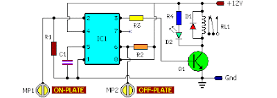
Component List 555 touch Switch
R1 = 3.3M
R2 = 3.3M
R3 = 10K
R4 = 1K
C1 = 10nF-63V
D1 = 1N4007
D2 = Red LED
Q1 = BC547
IC1 = NE555
RL1 = 12V Relay

Monday, January 20, 2014
Electronic Thermostat and Relay
Here is a simple thermostat circuit that can be used to control a relay and supply power to a small space heater through the relay contacts. The relay contacts should be rated above the current requirements for the heater. Temperature changes are detected by a (1.7K @ 70F) thermistor placed in series with a 5K potentiometer which produces about 50 millivolts per degree F at the input of the LM339 voltage comparator. The two 1K resistors connected to pin 7 set the reference voltage at half the supply voltage and the hysteresis range to about 3 degrees or 150 millivolts. The hysteresis range (temperature range where the relay engages and disengages) can be adjusted with the 10K resistor between pins 1 and 7. A higher value will narrow the range.
Electronic Thermostat and Relay Circuit Diagram
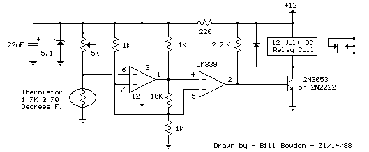
In operation, the series resistor is adjusted so that the relay just toggles off at the desired temperature. A three degree drop in temperature should cause the relay to toggle back on and remain on until the temperature again rises to the preset level. The relay action can be reversed so it toggles off at the lower end of the range by reversing the locations of the 5K potentiometer and thermistor. The 5.1 volt zener diode regulates the circuit voltage so that small changes in the 12 volt supply will not effect operation. The voltage across the thermistor should be half the supply or about 2.6 volts when the temperature is within the 3 degree range set by the potentiometer. Most any thermistor can be used, but the resistance should be above 1K ohm at the temperature of interest. The series resistor selected should be about twice the resistance of the thermistor so the adjustment ends up near the center of the control.
Electronic Thermostat and Relay Circuit Diagram
In operation, the series resistor is adjusted so that the relay just toggles off at the desired temperature. A three degree drop in temperature should cause the relay to toggle back on and remain on until the temperature again rises to the preset level. The relay action can be reversed so it toggles off at the lower end of the range by reversing the locations of the 5K potentiometer and thermistor. The 5.1 volt zener diode regulates the circuit voltage so that small changes in the 12 volt supply will not effect operation. The voltage across the thermistor should be half the supply or about 2.6 volts when the temperature is within the 3 degree range set by the potentiometer. Most any thermistor can be used, but the resistance should be above 1K ohm at the temperature of interest. The series resistor selected should be about twice the resistance of the thermistor so the adjustment ends up near the center of the control.
Sunday, January 19, 2014
Booster BLW 60
In this post an opportunity, I upload booster BLW 60 which may be an inspiration to create home brew. Here I include a file layout that can be unlocked via software sprint layout. of course the software you can download here as well. ok g tuk need to talk at length, immediately wrote download the full data here

Saturday, January 18, 2014
4 5 Mhz Notch Filter Schematic
Component value sensitivity is extremely critical, as are temperature coefficients and matching of the components. Best performance is attained when perfectly matched components are used and when the gain of the amplifier is unity.
4.5 Mhz Notch Filter Schematic

To illustrate, the quality factor Q is very high as amplifier gain approaches 1 with all components matched (in fact, theoretically it approaches infinity) but decreases to about 12.5 with the amplifier gain at 0.98.
4.5 Mhz Notch Filter Schematic
Friday, January 17, 2014
Differential amplifier circuit
Differential amplifier is an amplifier that works by amplifying the signal of the difference of the two inputs. Here is a schematic drawing of a simple differential amplifier:
 |
| Differential amplifier |
The differential amplifier using components BJT (Bipolar Junction Transistor) which is identical / exactly the same as the amplifier. In the differential amplifier has two input signals (input) the V1 and V2. Under ideal conditions, when both inputs are identical (Vid = 0), then the output VOD = 0. This is because IB1 = IB2 that IC1 = IC2 IE1 = IE2 and. Therefore, the output voltage (VC1 and VC2) cost the same so that VOD = 0.
If there is a difference between the signals V1 and V2, then the Vid = V1 - V2. This will cause the difference between IB1 and IB2. With prices so different from the IC2 IC1, so price increases VOD in accordance with the strengthening of the transistors.
Reinforcement can be used to enlarge the two-level differential amplifier (cascade). Differential amplifier output is connected to the input differential amplifier is the next level. With such a large total gain (Ad) is the product of the first differential amplifier gain (VD1) and the strengthening of the second differential amplifier (Vd2).
In practice, the differential amplifier is preferred if only one output. So that is use the voltage between the output and earth (ground). To be able to produce an output voltage to earth (ground) is equal to the voltage between the two outputs (VOD), then one of the differential amplifier output of the second level is connecting with an emitter follower (emitter follower).
To obtain better performance, then the output of emitter follower configuration connected by a so-called totem-pole. By using this configuration, the output voltage can swing in a positive X to near VCC and prices can swing in a negative way to approach the price of VEE.
Thursday, January 16, 2014
2 X 50W ICs amplifier with STK4191
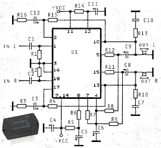
The above is a stereo amplifier circuit based on IC STK4191 with 2 X 50Watt output power 8 ohm impedance. And besides that you can use some of the IC can also be applied in this series include the STK4101, 4111, 4121, 5131, 4141, 4151, 5161, 4171, 4181, and 4191. Required supply voltage from 12 Volt to 35 Volt DC.Part List :
R1 = 22K
R2 = 22K
R3 = 560R
R4 = 56K
R5 = 1K
R6 = 1K
R7 = 100R
R8 = 2K
R9 = 2K
R10 = 4.7R
R11 = 2K2
R12 = 2K2
R13 = 4.7R
R14 = 100R
R15 = 56K
R16 = 560R
C1 = 0.1uF
C2 = 0.1uF
C3 = 100uF
C4 = 100uF
C5 = 100uF
C6 = 0.1uF
C7 = 47uF
C8 = 47uF
C9 = 0.1uF
C10 = 100uF
C11 = 100uF
U1 = STK4191
Wednesday, January 15, 2014
14 V battery charger circuit and troubleshooting
This circuit is also use operational amplifier IC LM324 to drive the VN64GA with the error signal and to control output voltage. This output voltage is pulsating DC , which is quite satisfactory for battery charging. This circuit also can be converted to the system regulated DC supply.
You do this by increased C2 and anoother electrolytic capacitor is added across the load. The respon time is very fast, determined by the op amp.
Schematic and troubleshooting below :

- AC cable disconnected
- Transformer is damaged or leaking.
- Broken or leaky diode.
- Installation of inverted foot elco.
- Instrallation of the components of the upside , particularly on the transistor , examine the placement of the feet emitter , collector and base.
- IC damaged.
- Soldering is less sticky.
- Line PCB damaged.
Subscribe to:
Posts (Atom)