Showing posts with label circuit. Show all posts

Saturday, October 25, 2014

Transformer Less Power Supply Circuit Diagram

This clever design uses 4 diodes in a bridge to produce a fixed voltage power supply capable of supplying 35mA. All diodes (every type of diode) are zener diodes. They all break down at a particular voltage. The fact is, a power diode breaks down at 100v or 400v and its zener characteristic is not useful.  But if we put 2 zener diodes in a bridge with two ordinary power diodes, the bridge will break-down at the voltage of the zener. This is what we have done. If we use 18v zeners, the output will be 17v4.
When the incoming voltage is positive at the top, the left zener provides 18v limit (and the left power-diode produces a drop of 0.6v).  This allows the right zener to pass current just like a normal diode but the voltage available to it is just 18v.  The output of the right zener is 17v4. The same with the other half-cycle.  The current is limited by the value of the X2 capacitor and this is 7mA for each 100n when in full-wave (as per thiscircuit). We have 10 x 100n = 1u capacitance. Theoretically the circuit will supply 70mA but we found it will only deliver 35mA before the output drops. The capacitor should comply with X1 or X2 class. The 10R is a safety-fuse resistor.
Circuit diagram:
TransformerLess Power-Supply-Circuit-Diagram
TransformerLess Power Supply Circuit Diagram 
The problem with this power supply is the "live" nature of the negative rail. When the power supply is connected as shown, the negative rail is 0.7v above neutral. If the mains is reversed, the negative rail is 340v (peak) above neutral and this will kill you as the current will flow through the diode and be lethal. You need to touch the negative rail (or the positive rail) and any earthed device such as a toaster to get killed. The only solution is the project being powered must be totally enclosed in a box with no outputs. 
Continue[...]

Friday, October 17, 2014

Fog Lamp Sensor Circuit Diagram

For several years now, a rear fog lamp has been mandatory for trailers and caravans in order to improve visibility under foggy conditions.
Circuit diagram :
Fog Lamp Sensor-Circuit Diagram
Fog Lamp Sensor Circuit Diagram
When this fog lamp is switched on, the fog lamp of the pulling vehicle must be switched off to avoid irritating reflections. For this purpose, a mechanical switch is now built into the 13-way female connector in order to switch off the fog lamp of the pulling vehicle and switch on the fog lamp of the trailer or caravan. For anyone who uses a 7-way connector, this switching can also be implemented electronically with the aid of the circuit illustrated here.
Here a type P521 optocoupler detects whether the fog lamp of the caravan or trailer is connected. If the fog lamp is switched on in the car, a current flows through the caravan fog lamp via diodes D1 and D2. This causes the LED in the optocoupler to light up, with the result that the phototransistor conducts and energises the relay via transistor T1. The relay switches off the fog lamp of the car.
For anyone who’s not all thumbs, this small circuit can easily be built on a small piece of perforated circuit board and then fitted somewhere close to the rear lamp fitting of the pulling vehicle.
Continue[...]

Para saki the QRP Transceiver fact Diodes Circuit Diagram

This circuit is a dream of 40 years was conducted, a transceiver QRP (low power) done without transistors, IC or valves, its creator just used diodes. The receiver has little gain, but works well for strong signals via the audio amplifier which is very effective.I believe this transceiver is at least very curious, though precarious it sure works and shows that the electron has no limits.

Para-saki the QRP Transceiver fact Diodes Circuit Diagram


Parasaki the QRP Transceiver fact Diodes Circuit Diagram
Continue[...]

Small Circuit Multiband Radio Transmitter CW


Small Circuit Multiband Radio - Transmitter CW

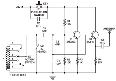
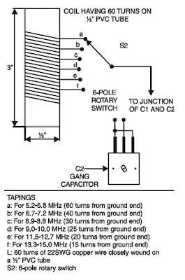
This is a Small Circuit Multiband Radio -Transmitter CW for who wants to learn more about radiofrequency, mainly operating principle from radios transceivers multiband, That circuit consists of a frequency oscillator RF, which is the main component us transmitters and radio receivers. 

He oscillates for high frequency, he is called variable frequency oscillator or VFO, their frequency may vary of 5.2 MHz to 15 MHz, depending the coil chosen and signal can be received in the band shortwave by any receiver radio.In S1 is used a switch type bell, but can-if use a handler CW, these used by radio amateurs. How antenna should-if use a the type dipole from 1/4 wave.

Small Circuit Multiband Radio - Transmitter CW


Continue[...]

Saturday, January 25, 2014

Elco tester circuit

elco capastor tester
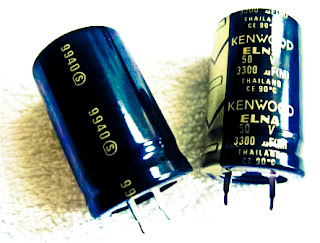
Elco testing small to use AVO meters. But to distinguish between the elco elco 20.000uF/50V 2200uF/50V size would be very difficult, perhaps this phenomenon that makes creative hands itch to make elco with two label values.


Scheme tool as follows, do not smile once, indeed simple. The cost to make it too cheap, not up to $ 1.

Elco tester circuit
Elco tester circuit

The workings of this tool based on the nature of the condenser, the condenser ability to store electrons / voltage. Since each condenser has the characteristic charging time and discharging time is different for each size and type dielektrika. Ideally, the larger size, the greater the time required for charging and discharging (charging and disposal charges).
How to use:

  • Make sure the position of the switch (SW1) on the discharging position (position A).
  • Connect / elco pairs that will be tested, then empty the contents briefly elco by pressing SW2 (approximately 1 to 3 seconds).
  • Position the switch in the charging position (position B), the LED will light with a certain time (depending on the value elco). Hold in position B until the LED is not lit (elco is full).
  • When the LED is not lit, immediately moved to the position of discharging position (A), the LED will light with a certain time (depending on the value elco tested). Hold in position A until the LED does not turn on again (fill elco is empty).
  • The conclusion is quite simple, the larger the size elco, the longer the charging time and dischargingnya (old LED lights up). To calibrate it, readers can use the benchmark elco 10000uF size that can be justified. Only by logic alone writers think readers have understood.
If it is the process of charging and discharging too quickly, the reader can change the value of R1, the greater the value the longer the charging process and discharging.

Good luck and commanded me, the value of its components should not be deleted, do not be wrapped up neatly, keep the same cast in epoxy / cement.
Continue[...]

Friday, January 24, 2014

Digital Bike Tachometer Circuit


This digital DIY tachometer for bikes uses two reed switches to get the speed information of the bicycle. The reed switches are installed near the rim of the wheel where permanent magnets pass by. The permanent magnets are attached to the wheelspokes and activate the reed switches everytime they pass by it. The speed is digitally displayed.

Electronic bicycle DIY tachometer circuit diagram
Digital Bike Tachometer

The tachometer circuit works according to this principle; the pulses created by the reed contacts are counted within a certain time interval. The resulting count is then displayed and represents the speed of the bike. Two 4026 ICs are used to count the pulses, decode the counter and control two 7-segment LED display. RS flip-flops U3 and U4 function as anti-bounce.

The pulses arrive at the counter’s input through gate U7. The measuring period is determined by monostable multivibrator U5/U6 and can be adjusted through potentiometer P1 so that the tacho can be calibrated. The circuit U1/U2 resets the counters.

Since batteries are used to power the circuit, it is not practical to support the continous display of speed information. This circuit is not continously active. The circuit is activated only after a button is pressed. At least three permanent magnets must be installed on the wheel. The circuit can be calibrated with the help of another precalibrated tachometer.
Continue[...]

Friday, January 17, 2014

Differential amplifier circuit

Differential amplifier is an amplifier that works by amplifying the signal of the difference of the two inputs. Here is a schematic drawing of a simple differential amplifier:

differential amplifier circuit diagram
Differential amplifier
The differential amplifier using components BJT (Bipolar Junction Transistor) which is identical / exactly the same as the amplifier. In the differential amplifier has two input signals (input) the V1 and V2. Under ideal conditions, when both inputs are identical (Vid = 0), then the output VOD = 0. This is because IB1 = IB2 that IC1 = IC2 IE1 = IE2 and. Therefore, the output voltage (VC1 and VC2) cost the same so that VOD = 0.

If there is a difference between the signals V1 and V2, then the Vid = V1 - V2. This will cause the difference between IB1 and IB2. With prices so different from the IC2 IC1, so price increases VOD in accordance with the strengthening of the transistors.

Reinforcement can be used to enlarge the two-level differential amplifier (cascade). Differential amplifier output is connected to the input differential amplifier is the next level. With such a large total gain (Ad) is the product of the first differential amplifier gain (VD1) and the strengthening of the second differential amplifier (Vd2).

In practice, the differential amplifier is preferred if only one output. So that  is use the voltage between the output and earth (ground). To be able to produce an output voltage to earth (ground) is equal to the voltage between the two outputs (VOD), then one of the differential amplifier output of the second level is connecting with an emitter follower (emitter follower).

To obtain better performance, then the output of emitter follower configuration connected by a so-called totem-pole. By using this configuration, the output voltage can swing in a positive X to near VCC and prices can swing in a negative way to approach the price of VEE.
Continue[...]

Wednesday, January 15, 2014

14 V battery charger circuit and troubleshooting

This circuit is also use operational amplifier IC LM324 to drive the VN64GA with the error signal and to control output voltage. This output voltage is pulsating DC , which is quite satisfactory for battery charging. This circuit also can be converted to the system regulated DC supply.
You do this by increased C2 and anoother electrolytic capacitor is added across the load. The respon time is very fast, determined by the op amp.
Schematic and troubleshooting below :
If the circuit not work , Perhaps the cause of :
  • AC cable disconnected
  • Transformer is damaged or leaking.
  •  Broken or leaky diode.
  • Installation of inverted foot elco.
  • Instrallation of the components of the upside , particularly on the transistor , examine the placement of the feet emitter , collector and base.
  • IC damaged.
  • Soldering is less sticky.
  • Line PCB damaged.
Continue[...]

Tuesday, January 14, 2014

SMS Remote controller circuit

SMS Remote controller is a device used to control a device remotely using SMS through GSM mobile phones. Process control equipment with a series of AVR ATTiny To SMS Remote Controller can be used to control life and death of these equipment will provide information on the status of replies to our phone in return successful command execution. 
Equipment can be controlled by a series of AVR ATTiny To SMS Remote Controller include lights, water pumps, garage doors, gates and much more. AVR series ATTiny To SMS Remote controller uses the module-47 Sony ericson GM as recipient and sender of the SMS module. Then to the SMS data processor on a series of AVR ATTiny To SMS Remote controller is using AVR microcontroller ATTiny 2313.


Series AVR ATTiny To SMS Remote Controller

SMS Remote controller circuit Click to view larger. 

AVR circuit this part ATTiny To SMS Remote Controller
AVR series ATTiny To SMS Remote controller uses the AVR attiny2313 with 4MHz clock frequency, GSM Module GM trnceiver 47 Sony ericson, SIM Card, 4 relays and an IC regulator. ATTiny AVR microcontroller 2313 can work well on the voltage 2.7 VDC - 5.5 VDC for working with the frequency at 10MHz bahwah. 

The set of AVR ATTiny In SMS Remote Controller To make use of this power supply from the batteries 3.3 VDC. Connection using a SIM Card SIM Card Holder which is connected to the module GM-47, AVR series ATTiny To SMS Remote Controller works with communication between AVR ATTiny and GM-47 module at 9600bps. In a series of AVR ATTiny To SMS Remote controller is equipped with LED D6 as an indicator of the data interconnect GM-47 module with cellular operators where this LED will light continuously when not apat network and will be lit by flashes when a signal from the operator.

Specs AVR series ATTiny To SMS Remote Controller


  • 4 Relay for ON / OFF electronic devices
  • 8 input lines for reading in a normal switching
  • LED indicators signal operator
  • SMS command with password, so only the owner can operate
Continue[...]

Saturday, January 11, 2014

Control Relay Circuit with 9 Second

See figure below its Control Relay Circuit Schematics.


Control Relay Circuit
Continue[...]

Friday, January 10, 2014

Audio Stereo Channel Selector Circuit

Audio Stereo Channel Selector CircuitAudio Stereo Channel Selector Circuit

This circuit has accouterment for abutting stereo outputs from four altered sources/channels as inputs and alone one of them is selected/connected to the achievement at any one time.

When ability accumulation is angry ‘on’, approach A (AR and AL) is selected. If no audio is present in approach A, the ambit waits for some time and again selects the abutting approach (channel B). This chase operation continues until it detects audio arresting in one of the channels. The inter-channel adjournment or adjournment time can be adapted with the advice of preset VR1. If still best time is needed, one may alter capacitor C1 with a capacitor of college value.

Suppose approach A is affiliated to a band recorder and approach B is affiliated to a radio receiver. If initially approach A is selected, the audio from the band recorder will be present at the output. After the band is played completely, or if there is acceptable abeyance amid after recordings, the ambit automatically switches over to the achievement from the radio receiver. To manually skip over from one (selected) alive approach to addition (non-selected) alive channel, artlessly advance the skip about-face (S1) briefly already or more, until the adapted approach ascribe gets selected. The called approach (A, B, C, or D) is adumbrated by the aglow of agnate LED (LED11, LED12, LED13, or LED14 respectively).

IC CD4066 contains four alternation switches. These switches are affiliated to four abstracted channels. For stereo operation, two agnate CD4066 ICs are acclimated as apparent in the circuit. These alternation switches are controlled by IC CD4017 outputs. CD4017 is a 10-bit arena adverse IC. Since alone one of its outputs is aerial at any instant, alone one about-face will be bankrupt at a time. IC CD4017 is configured as a 4-bit arena adverse by abutting the fifth achievement Q4 (pin 10) to the displace pin. Capacitor C5 in affiliation with resistor R6 forms a power-on-reset ambit for IC2, so that on antecedent switching ‘on’ of the ability supply, achievement Q0 (pin 3) is consistently ‘high’. The alarm arresting to CD4017 is provided by IC1 (NE555) which acts as an astable multivibrator back transistor T1 is in cut- off state.

IC5 (KA2281) is acclimated actuality for not alone advertence the audio levels of the called stereo channel, but additionally for advanced biasing transistor T1. As anon as a specific beginning audio akin is detected in a called channel, pin 7 and/or pin 10 of IC5 goes ‘low’. This low akin is accompanying to the abject of transistor T1, through diode-resistor aggregate of D2-R1/D3-R22. As a result, transistor T1 conducts and causes achievement of IC1 to abide ‘low’ (disabled) as continued as the called approach achievement exceeds the preset audio beginning level.

Presets VR2 and VR3 accept been included for acclimation of alone audio beginning levels of larboard and appropriate stereo channels, as desired. Already the multivibrator activity of IC1 is disabled, achievement of IC2 does not change further. Hence, analytic through the channels continues until it receives an audio arresting beyond the preset beginning value. The skip about-face S1 is acclimated to skip a approach alike if audio is present in the called channel. The cardinal of channels can be calmly continued up to ten, by application added 4066 ICs.

Continue[...]

Friday, December 27, 2013

Video IF circuit TV

Video IF circuit
Video IF circuit
The main function of the video IF is to change the 38.0 MHz IF signal into the CVBS signal which later fed into the sound and video to the chroma.


VIF section consists of a series as follows:
IF amplifier
This section serves to strengthen the signal until the signal level is required. IF amplifier is equipped with AGC (Automatic Gain Controller) which controls the strengthening of the IF amplifier so that a constant amplitude output video. Amplifier frequency range from 32 ~ 60 MHz makes this amplifier suitable for applications multistandar.

PLL demodulator and VCO (voltage control oscillator)
IF signal is separated with the help of PLL detector. PLL detector produces a phase reference signal with the IF signal carrier and about 60 KHz bandwidth is determined by PLL loopfilter pin 37. Obtained by comparing the frequency demodulation reference signal with the incoming IF signal. Are required reference frequency (38.0 MHz) generated by the VCO. Appropriate VCO frequency is determined by system calibration using the crystal as a reference. PLL can detect the IF frequency up to ± 1 MHz based on FPLL (Frequency Phase Lock Loop System) which will provide an output signal to the PLL loopfilter for the difference frequency is obtained. If the phase IF signal with a reference signal, the signal is transmitted to the demodulator. Demodulator to control the positive and negative modulation, the selection made ​​by the IIC bus. Low pass filter after the output signal demodulator eliminates the demodulation is not required to process the video.

Video IF schematics


Video Buffer
Video buffer to produce a video output with an amplitude of the right and keep the video output from the noise peak occurring. The bandwidth of the video buffer at least 6 MHz. In the video there are White spot clamp buffer (for positive modulation) and the noise inverter Clamp (for negative modulation) which keeps the amplitude of the video does not exceed the typical price.

Continue[...]

Thursday, December 26, 2013

A 4 Digit Keypad Controller Switch Circuit

A 4-Digit Keypad Controller Switch CircuitA 4-Digit Keypad Controller Switch Circuit

This is a universal version of the Four-Digit Alarm Keypad . I have modified the design to free up the relay contacts. This allows the circuit to operate as a general-purpose switch. It also means that it can be used to control all of my Alarm Circuits. Ive used a SPCO/SPDT relay - but you can use a multi-pole relay if you wish.

The relay is energized by pressing a single key. Choose the key you want to use - and connect it to terminal "E". Choose the four keys you want to use to de-energize the relay - and connect them to "A B C & D". Wire the common to R1 and all the remaining keys to "F".

The Circuit is easy to use. When you press "E" - current through D2 & R9 turns Q6 on - and energizes the relay. The two transistors - Q5 & Q6 - form a "Complementary Latch". So - when you release the key - the relay will remain energized.

To de-energize the relay - you need to press keys "A B C & D" in the right order. When you do so - pin 10 of the IC goes high - and it turns Q4 on through R8. Q4 connects the base of Q6 to ground. This unlatches the complementary pair - and the relay drops out.

Any keys not wired to "A B C D & E" are connected to the base of Q3 by R7. Whenever one of these "Wrong" keys is pressed - Q3 takes pin 1 low and the code entry sequence fails. If "C" or "D" is pressed out of sequence - Q1 or Q2 will also take pin 1 low - with the same result. If you make a mistake while entering the code - simply start again.

The Keypad must be the kind with a common terminal and a separate connection for each key. On a 12-key pad, look for 13 terminals. The matrix type with 7 or 8 terminals will NOT do. With a 12-key pad - over 10 000 different codes are available. If you need a more secure code - use a bigger keypad with more "Wrong" keys wired to "F". A 16-key pad gives over 40 000 different codes.
Continue[...]

Sunday, December 22, 2013

Car Battery Charger 12Volt Circuit Diagram

Car Battery Charger 12Volt Circuit DiagramCar Battery Charger 12Volt Circuit Diagram

The aloft circuit claimed accept adeptness to anticipate array blackmail that accomplish electrolyte absent due to evaporation. This ambit will annihilate the problems by ecology the battery’s action of allegation through its attendant ascendancy ambit by applying a aerial allegation accepted until the array is absolutely charged. Back charging is complete, it turns on the red LED (LD2) and deactivates the charging circuit.

This ambit is fatigued to allegation 12V batteries ONLY. Certain accent should be taken back base up this circuit. They are the access of the agent to the ambit board, and those bartering accepted to the array actuality charged. These access should be fabricated with cables accepting a ample cross-sectional breadth to anticipate voltage-drop and calefaction accession back accepted flows through them.

Continue[...]

Tuesday, December 17, 2013

50MW Audio Amplifier circuit

50MW Audio Amplifier circuit50MW Audio Amplifier circuit

The following is a small audio amplifier comparable to what you may come across a small transistor radio medium size. The input stage is biased to ensure that the power is divided equally to provide the two complimentary output transistors which are slightly biased in conduction of the diodes between the bases. A 3.three ohm used in sequence for the use of the issuers of the output transistors to stabilize the bias current that does not change significantly with temperature or several transistors and diodes.

Due to recent increases in bias voltage between the emitter and base decreases as a result of minimizing driving. Input impedance is 500 ohms and the voltage gain is approximately five to eight ohm speaker connected. The voltage swing around the speaker is 2 volts without distorting production and capacity is at the same time in the 50 milliwatt range. A high voltage provided as well as the addition of heat sinks in the output transistors would be a great source of more power. Circuit thirty milliamperes draw a supply of 9 volts.
Continue[...]

Monday, December 9, 2013

Battery charger circuit

This cahrger based on chargeing voltage 2,4 Volts per cell , in accordance with most manufacterers recomendation. This circuit pulses the battery under with 14.4 Volts ( 6 cells x 2,4 volts per cell) at a rate 120 Hz.
Continue[...]

Friday, December 6, 2013

Reducing Treble tone circuit

Treble reducer circuit above is an example of a simple circuit and is suitable to be used as experimental material and analysis of the workings of the circuit. 


As I mentioned earlier the bass reducer series, this series actually has the same working principles with a series of bass reducer. Where these circuits utilize capacitors nature of the charge and discharge. The difference of the damping function obtained from the difference of the capacitor. If the series bass reducer series capacitors are mounted on the op-amp input lines, while in this treble reducer series capacitors are mounted parallel with the strengthening of the op-amp prisoners. Installation of this circuit has a parallel in the work analysis in contrast with the installation of the series on a series of bass reducer. The difference is that the installation of the series, so we URLs that are easy to understand how a wire working capacitors for high frequency signal, so with high frekuesni so automatic signal to be passed to the output terminal by a capacitor. But if we put a parallel between the output capacitor with the terminals, then automatically because the capacitor is considered as a wire so the voltage on the capacitor is near 0 volts, so the output voltage will also follow the voltage on the capacitor because they connect parallel. As with the low frequency signal, the capacitor is considered open and makes voltage wire that fell to him is to approach the input voltage. To understand how the capacitor can be regarded as a wire or an open switch I mentioned in my post about the working principles of capacitors and a series of bass reducer.

Indeed, when examined in detail, not only the capacitors that play a role here but the component resistors and op-amp also affect. But I can confirm that the main function is performed by a capacitor reduction. Series resistors are intended to be installed that will flow into the capacitor can be adjusted so that it influences the charge and discharge the capacitor will make the appropriate damping.

Take a look at the picture above the treble reducer circuit and also the image output signal. There are two function generator as input and has a signal with different frequencies. The first signal of amplitude 1 volt and low frequencies, the two signals with an amplitude of 1 volt and with high frequency. At the time of our input select switch position to the relationship with the input low frequency signal, the signal output will be nearly equal to the input signal such as no change. Whereas if we switch position to link high-frequency input signal then the output signal amplitude will be damped near 0 volts.

Example treble reducer circuit is very simple and can you develop more in accordance with the desires and your needs. At least with understanding the working principle of this circuit we can apply a time when we are required to perform the function of damping trebele.
Continue[...]

Thursday, December 5, 2013

Quad Audio Amplifier Circuit diagram with TDA7831 4×25W

Quad Audio Amplifier Circuit diagram with TDA7831 4×25WQuad Audio Amplifier Circuit diagram with TDA7831 4×25W


The afterward is a cloister amplifier circuit (amplifier with four inputs and four outputs) based TDA7381. This amplifier is advised for car audio system, but you can additionally use this ambit for added purposes. This ambit has a architecture actual simple and actual accessible to build.
Continue[...]

Monday, December 2, 2013

Black Box Lightshow Circuit

Black Box Lightshow Circuit Heres the circuit for the Black Box Lightshow. Im pretty sure its right. And now, an explanation: The LED array is shown here as individual diodes, though I used six 5x7 LED arrays, each one is 2" tall.

Black Box Lightshow Circuit

They are arranged as 14 rows and 15 columns. The left channel is 8 columns and the right channel is 7 columns. The extra column from the left channel is the center column and gives nice symmetry. Not shown here is that on the right channel, the first column (pin 1) is not used so that the other columns are equal. The LM3914 is a Dot/Bar Display Driver. 

It does all the heavy lifting of converting the audio signal into a series of bars - these are typically used as digital meters. The potentiometer sets the sensitivity of the display. Since the rows are multiplexed (see below), each column is only driving one LED at a time. I only show the left channel here, the right channel is identical, and they share the level setting potentiometer. The right portion of the diagram is a 555 clock, a 7493 4-bit counter and a 74154 4-to-16 line decoder/demultiplexer. 

This is the "sweep" part of the display that cycles through each row of LEDs. The potentiometer at the top controls the sweep speed. The net result is that the 74154 is cycling through the pins/rows, grounding each in succession. Note that I only have 14 rows, but it is counting to 16 each time. No big deal, it doesnt affect the perceived output at all. The N2907 transistors are there to provide enough power for all the LEDs. Potentially, all 15 LEDs in a row can be lit up at once, so the transistors make sure there is enough juice. Unfortunately, I lost the original plans during a garage cleaning after I built the electronics (the box took another few months before I got around to it). I opened it up and reverse engineered my own work. I wont guarantee it, but it sure looks right to me. The one weird thing I found is that I dont have power going to pin 8 of the 555 (as shown here), but it works fine - go figure. Also, Im not 100% sure I got the polarity of the LEDs right, sorry about that. I would recommend testing that out first.
Continue[...]

Saturday, November 30, 2013

6 Watt Audio Amplifier Schematic Circuit with TDA1519

6 Watt Audio Amplifier Schematic Circuit with TDA15196 Watt Audio Amplifier Schematic Circuit with TDA1519

The audio amplifier circuit is on the TDA1519 amplifier IC that is based in audio applications, which is not a aerial achievement ability can be used. The ambit TDA1519 is a ability of 2×6 watts.

The TDA1519 is an amplifier congenital Class B dual-output advance in a 9-by-line (SIL) artificial amalgamation boilerplate achievement is primarily developed for car radio applications.

Key Features of the audio amplifier IC TDA1519 are: Requires few alien components, anchored gain, acceptable bounce drive, aphasiac / standby mode, thermal protection, about-face polarity safe. Tda1519 amplifier ability rating, 14.4 volts.

Continue[...]