Showing posts with label radio. Show all posts
Showing posts with label radio. Show all posts
Friday, October 17, 2014
Small Circuit Multiband Radio Transmitter CW
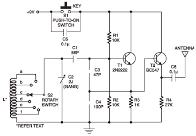
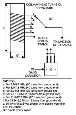
This is a Small Circuit Multiband Radio -Transmitter CW for who wants to learn more about radiofrequency, mainly operating principle from radios transceivers multiband, That circuit consists of a frequency oscillator RF, which is the main component us transmitters and radio receivers.
He oscillates for high frequency, he is called variable frequency oscillator or VFO, their frequency may vary of 5.2 MHz to 15 MHz, depending the coil chosen and signal can be received in the band shortwave by any receiver radio.In S1 is used a switch type bell, but can-if use a handler CW, these used by radio amateurs. How antenna should-if use a the type dipole from 1/4 wave.

Thursday, January 23, 2014
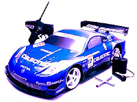
Radio remote controls for toy cars
In this system, radio signals are not transmitted continuously but only generated when the controller sends a command to the left / right or forward / backward, and even then only a radio-frequency discontinuous, so is sending pulses of radio wave frequency.
The number of pulses sent represent commands sent, GO command is represented with 8 pulses, is represented with 16 pulses LEFT, RIGHT DOWN 32 pulses and 64 pulses. Commands that can dikirimk is a combination of 2 orders once gus, which is a combination of command forward / backward and right / left, for example, could be sent forward orders and left once gus, in this case the number of pulses sent is 24, ie the sum of the forward command by 8 pulse and left the command of 16 pulses.
After a command is sent, the system stops sending commands in a certain time lag, the lag time it takes will be a series of recipients have sufficient time to fulfilling their orders well. Frequency pulses were visible on the right side of this.
 |
| Radio Control Transmitter Series |
How it works Transmitter
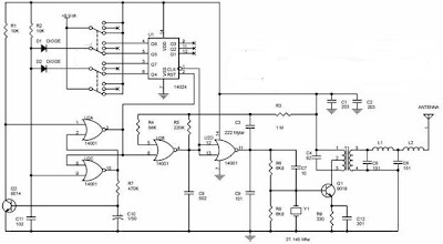
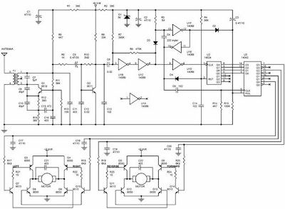
Radio signals generated by oscillator circuit formed by transistors Q1 9016, the working frequency of the oscillator is determined by the crystal Y1 is worth 27.145 MHz. A very critical part of this oscillator circuit is T1, L1 and L2, which specifically dealt with separately at the end of this article. Working from this oscillator is controlled by NOR gate U2D 14001, while the output gate (pin 3) is worth 1, the oscillator will work and transmit radio frequency 27.145 MHz, and at the output U2D value 0 the oscillator will stop working. U2D NOR gate receives the clock signal from NOR gate U2B. NOR Gate CMOS type with the aid of resistors R4 and R5 and capacitor C8 form a low frequency oscillator circuit for controlling the clock shaper of existing digital circuits. Work of this clock generator is controlled via the input leg 6, the circuit will generate the clock if this input berlevel 0 .
NOR gate U2A and U2C form a series of Latch (RS Flip Flop), because of the influence of the resistor R2 and capacitor C11 is fed to pin 9 in U2C, when the circuit gets power supply output U2C must be 1 and the output of U2A (leg number 3) becomes 0 . This situation resulted Marja U2b clock generator works evoke reset the clock and remove the state of the enumerator 14 024 IC (U1), so that U1 started chopping and 27.145 MHz oscillator circuit sending pulses for generating a clock frequency of work.
At the start chopping, all the output of IC 14 024 enumerators in kedaan 0 , after chopping 8 Q4 output pulse (pin 6) will be a 1, after counting 16 pulses output Q5 (pin 5) to 1 , after chopping 32 Q6 output pulse (pin 4) to 1 , after counting 64 pulses output Q7 (pin 3) to 1.
Output over-output voltage used to control foot 9 U2C through diode D1 and D2, during one of the output is still worth 0 then the clock generator U2B still working, this will continue until the cathode D1 D2 dankatode be 1 so that the foot 9 U2C be a 1 as well. This situation will result in the output feet 3 U2A to 1 , which stop the clock generator U2B and resets the enumerator 14 024 danberhenti already shipping 27 145 MHz pulse frequency.
To generate the lag time for receiver circuit has enough time carrying out orders, used a series of Q2 9014, resistor R7 and capacitor C10. The amount of delay time is determined by the value of R7 and C10. Switch to send command forward / backward and to send commands left / right are two separate switches. Each switch has 3 positions, the center position means that the scalar does not send commands.
 |
| Radio Control Receiver series |
How it works Receiver
Figure 2 is a picture that matched the car receiver circuit toy, serves to receive signals from the transmitter to control motor cars, so cars can move forward / backward and left / right. Transistor Q1 with the help of resistors, capacitors and T1 form as a series of radio signal receiver 27.145 MHz. T1 in this series exactly the same as T1 that is used in the transmitter circuit, means of manufacture are discussed below.
Transistor Q2 follows perlangkapannya forming circuit to convert the radio frequency pulses received from the transmitter into the box pulses that can be accepted as a digital signal by the CMOS IC. Digital signal will be received as the clock had to be chopped by chopper 14 024 IC (U2). Output 14 024 will be in accordance with the number of pulses sent by the transmitter, forward command and left (which is used as an example in the discussion of the transmitter) is the pulse number of 24, the results of counting these pulses cause the output to be 14 024 Q4 = 1 , Q5 = 1, Q6 = 0 and Q7 = 0.
Digital signal received in addition be used as a clock IC 14 024 enumerators U2 discussed above, used also to drive the 3 pieces of the time delay circuit to generate pulses which controls the circuit work.
Toll regulator will first appear after delivery frequency pulse stopped because the lag time between sending the code, this pulse serves to record the count results to the U3 14 024 14 042 (D Flip Flop), making the final conditions of 14 024 will be retained to control the motor. After the results were recorded to 14 024 14 042, 14 042 enumerator is reset by the second pulse, after the lag time for 14,042 enumerators can count start from 0 again.
The circuit formed by transistors Q3, Q4, Q7, Q8, Q9 and Q10 named as H Bridge circuit, this circuit is very reliable to drive DC motors. With this series of DC motor can be rotated to the right-to-left or stop motion. The main requirement of the use of this circuit is the base voltage of Q7 and Q10 base voltage must be opposed, for example base Q7 = 1 and the base of Q10 = 0 the motor rotates to the left, the base of Q7 = 0 and the base of Q10 = 1 the motor will spin to the right, the base Q7 = 0 and the base Q10 = 0 motor stop motion, but it should not happen, the base Q7 = 1 and the base of Q10 = 1.
Similarly, Q5, Q6, Q11, Q12, Q13 and Q14 form a H Bridge. H Bridge to the left in Figure 2 is used to control motors that adjust the cars moving left / right, while the H Bridge right part is used to control motors that regulate movement forward / backward cars. The relationship between outpur enumerator 14 042 and 14 024 Input D Flip Flop is structured so that the signal is fed to each H Bridge can not be all 1 simultaneously.
Making transformer TX and RX
Transformer T1 in series transmitter and receiver, is the same stuff, and have created their own. Transformer was built using plastic transformer Koker (spare part radio) that have a step that looks 5 lanes that can be filled with rolls of wire, as shown in the photo. Using this Koker facilitate wire transformer winding. If you can not Koker similar to it, just use the usual. Koker feritnya transformer is small and is also small (3 mm) as the first is often used for assembly of 27 MHz CB radio.
Wire to the transformer can wear a wire in the unloading of these Koker, carefully open coil of wire that already exist within the Koker because the wire is smooth and quite easy to break.
Step 1: Roll away from the feet of wire fed into the number 5 ft 4 in the direction h (CW) as much as 3 rolls right in level 1 (point level above the lowest point)
Step 2: Wind the wire from leg 1 to leg 2 in a clockwise direction as much as 4 rolls right on level 2.
Step 3: Continue the roll (from step 2) clockwise a quarter roll to as much as 3 feet 3 at level three. (Can be determined exactly a quarter of the roll, because kokernya have a path cut into 4).
Making coil L1
Wind the copper wire diameter of 0.3 to 0.5 mm by 10 quarter rolls on Koker diameter about 4 mm (which will be released), also in a clockwise direction.
Making coil L2
Wind the copper wire diameter of 0.1 mm by 50 rolls of plastic Koker without ferrite diameter of about 3.5 - 4 mm (look for plastic materials from used goods) are also in a clockwise direction. The length of the section in liputi rolls along the 5 mm.
Saturday, November 2, 2013
Power amplifier for FM radio receiver
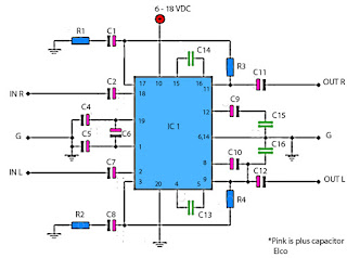
Schematic is suitable for use in radio tuner or FM radio receiver when it is assembled and ready for use. Where if the low gear power radio receiver, with the aid of power amplifier is less powerfull voice / hard to better and just right. For use hios speakers , use a low-power , because power amplifier has only the power output of 2 X 5 Watt stereo power amplifeir with impedance of 4 Ohm. Working on a minimum voltage of 4.5 Volts and maximum of 16Volt. Use the correct voltage supply - really have been filtered out in order to improve the performance of these power amplifiers.
Resistor
R1________180R
R2________180R
R3________18K
R4________18K
Capacitor
C1________47uF
C2________4.7uF
C4________100uF
C5________100uF
C6________47uF
C7________4.7uF
C8________47uF
C9________100uF
C10_______100uF
C11_______1000uF
C12_______1000uF
C13_______100pF
C14_______100pF
C15_______68n
C16_______68n
IC
IC1_______TA7215P
Sunday, December 30, 2012
CMOS Crystal Frequency Multiplier
Crystals usually operate at fundamental frequencies up to about 15 MHz. Whenever higher frequencies are required a frequency multiplier is placed after the crystal oscillator. The resulting output signal is then a whole multiple of the crystal frequency. Other frequency multipliers often use transistors, which produce harmonics due to their non-linearity. These are subsequently filtered from the signal. One way of doing this is to put a parallel L-C filter in the collector arm. This filter could then be tuned to three times the input frequency. A disadvantage is that such a circuit would quickly become quite substantial.
 This circuit contains only a single IC and a handful of passive components, and has a complete oscillator and two frequency triplers. The output is therefore a signal with a frequency that is 9 times as much as that of the crystal. Two gates from IC1, which contains six high-speed CMOS inverters, are used as an oscillator in combination with X1. This works at the fundamental frequency of the crystal and has a square wave at its output. A square wave can be considered as the sum of a fundamental sine wave plus an infinite number of odd multiples of that wave. The second stage has been tuned to the first odd multiple (3 x).
 We know that some of our readers will have noticed that the filter used here is a band-rejection (series LC) type. Worse still, when you calculate the rejection frequency you’ll find that it is equal to the fundamental crystal frequency! The fundamental frequency is therefore attenuated, which is good. But how is the third harmonic boosted? That is done by the smaller capacitor of 33 pF in combination with the inductor. Together they form the required band-pass filter. (The same applies to the 12 pF capacitor in the next stage.) Through the careful selection of components, this filter is therefore capable of rejecting the fundamental and boosting the third harmonic! Clever, isn’t it?.
 The output in this example is a signal of 30 MHz. The inverter following this stage heavily amplifies this signal and turns it into a square wave. The same trick is used again to create the final output signal of 3 times 30 MHz = 90 MHz. At 5 V this circuit delivers about 20 milliwatt into 50 R. This corresponds to +13 dBm and is in theory enough to drive a diode-ring balanced mixer directly. The circuit can be used for any output frequency up to about 100 MHz by varying the component values. When, for example, an 8 MHz crystal is used to obtain an output frequency of 72 MHz (9 x 8 = 72), the frequency determining inductors and capacitors have to be adjusted by a factor of 10/8.
You should round the values to the nearest value from the E12 series. Another application is for use in an FM transmitter; if you connect a varicap in series with the crystal, you can make an FM modulator. An added bonus here is that the relatively small modulation level is also increased by a factor of 9. Crystals with frequencies near 10 MHz are relatively easy to find and inexpensive, so you should always be able to find a suitable frequency within the FM band. A crystal of 10.245 MHz for instance would give you a frequency of 92.205 MHz and 10.700 MHz results in an output of 96.300 MHz. You may find that the circuit operates on the border of the HC specifications. If this causes any problems you should increase the supply voltage a little to 6V.
Continue[...]
 This circuit contains only a single IC and a handful of passive components, and has a complete oscillator and two frequency triplers. The output is therefore a signal with a frequency that is 9 times as much as that of the crystal. Two gates from IC1, which contains six high-speed CMOS inverters, are used as an oscillator in combination with X1. This works at the fundamental frequency of the crystal and has a square wave at its output. A square wave can be considered as the sum of a fundamental sine wave plus an infinite number of odd multiples of that wave. The second stage has been tuned to the first odd multiple (3 x).
 We know that some of our readers will have noticed that the filter used here is a band-rejection (series LC) type. Worse still, when you calculate the rejection frequency you’ll find that it is equal to the fundamental crystal frequency! The fundamental frequency is therefore attenuated, which is good. But how is the third harmonic boosted? That is done by the smaller capacitor of 33 pF in combination with the inductor. Together they form the required band-pass filter. (The same applies to the 12 pF capacitor in the next stage.) Through the careful selection of components, this filter is therefore capable of rejecting the fundamental and boosting the third harmonic! Clever, isn’t it?.
 The output in this example is a signal of 30 MHz. The inverter following this stage heavily amplifies this signal and turns it into a square wave. The same trick is used again to create the final output signal of 3 times 30 MHz = 90 MHz. At 5 V this circuit delivers about 20 milliwatt into 50 R. This corresponds to +13 dBm and is in theory enough to drive a diode-ring balanced mixer directly. The circuit can be used for any output frequency up to about 100 MHz by varying the component values. When, for example, an 8 MHz crystal is used to obtain an output frequency of 72 MHz (9 x 8 = 72), the frequency determining inductors and capacitors have to be adjusted by a factor of 10/8.
You should round the values to the nearest value from the E12 series. Another application is for use in an FM transmitter; if you connect a varicap in series with the crystal, you can make an FM modulator. An added bonus here is that the relatively small modulation level is also increased by a factor of 9. Crystals with frequencies near 10 MHz are relatively easy to find and inexpensive, so you should always be able to find a suitable frequency within the FM band. A crystal of 10.245 MHz for instance would give you a frequency of 92.205 MHz and 10.700 MHz results in an output of 96.300 MHz. You may find that the circuit operates on the border of the HC specifications. If this causes any problems you should increase the supply voltage a little to 6V.
Wednesday, October 24, 2012
1kH Synthetic Inductor
Inductors can be mimicked quite easily using operational amplifiers. The circuit shown here was developed to have an inductance of 1000 H (say, one thousand Henry) with good damping. Using this design you can build a resonant circuit with a center frequency of less than 1 Hz. The slow behavior allows you to use conventional measuring instruments to investigate the circuit in real time. The circuit can also be used as part of a filter design. Opamp1 operates as an Integrator, Opamp2 as a difference amplifier.
 The output voltage of Opamp2 is equal to the voltage drop across R1 and P1, which is proportional to the output current. This voltage is differentiated by Opamp1, C1 and R2. The net effect is that the circuit behaves as an inductor. P1 allows adjustment of the inductance value. P2 allows adjustment of the Q factor of the coil by altering the symmetry of the difference amplifier and with it the stability of the circuit.
Continue[...]
 The output voltage of Opamp2 is equal to the voltage drop across R1 and P1, which is proportional to the output current. This voltage is differentiated by Opamp1, C1 and R2. The net effect is that the circuit behaves as an inductor. P1 allows adjustment of the inductance value. P2 allows adjustment of the Q factor of the coil by altering the symmetry of the difference amplifier and with it the stability of the circuit.
Saturday, October 23, 2010
Wire Tracer (Transmitter)
The circuit depicted here forms one half of a device that will prove extremely handy when tracing the path of electrical wiring in a building or to locate a break in a wire. The system is based on similar equipment that is used by technicians in telephone exchanges. The operation is straightforward. You require a generator that delivers an easily recognizable signal which, using a short antenna, is inductively coupled to a simple, but high gain, receiver. To create a useful transmitter it would suffice to build a simple generator based on a 555. But as the adjacent diagram shows, a 556 was selected instead. The second timer (IC1a) is used to modulate the tone produced by IC1b.
 The output frequency alternates between about 2100 Hz and 2200 Hz. This is a very distinctive test signal that is easily distinguished from any other signals that may be present. Resistor R6 is connected to a piece of wire, about ten centimeters long, that functions as the antenna. The ground connection (junction C2-C3) is connected to ground. When the antenna is connected directly to a cable, it is possible to determine at the other end of the cable, with the aid of the receiver, which conductor is which (don’t do this with live conductors!). The schematic for the matching receiver may be found elsewhere in this website.
Continue[...]
 The output frequency alternates between about 2100 Hz and 2200 Hz. This is a very distinctive test signal that is easily distinguished from any other signals that may be present. Resistor R6 is connected to a piece of wire, about ten centimeters long, that functions as the antenna. The ground connection (junction C2-C3) is connected to ground. When the antenna is connected directly to a cable, it is possible to determine at the other end of the cable, with the aid of the receiver, which conductor is which (don’t do this with live conductors!). The schematic for the matching receiver may be found elsewhere in this website.
Wire Tracer (Receiver)
The circuit depicted is the receiver device of a transmitter/receiver combination that will prove extremely handy when tracing the path of electrical wiring in a building or to locate a break in a wire. The corresponding transmitter may be found elsewhere in this website. The transmitter produces a distinctive tone which alternates between 2100 Hz and 2200 Hz. The matching receiver for the wire tracer is possibly even simpler than the transmitter, as is shown by the schematic. It consists of no more than a short wire antenna (a piece of wire, 10 cm long is adequate), a high-pass filter (C1-R1), an amplifier stage (IC1), an output stage (T1) and a loudspeaker.
 The prototype used a high impedance loudspeaker from a telephone handset, and this worked remarkably well. The purpose of P1 is to adjust the amplification. At the highest amplification, the wire energized by the transmitter can be traced from several tens of centimeters away. A direct electrical connection is therefore not required. However, it is important that you hold the ground connection (earth) in your hand.
Continue[...]
 The prototype used a high impedance loudspeaker from a telephone handset, and this worked remarkably well. The purpose of P1 is to adjust the amplification. At the highest amplification, the wire energized by the transmitter can be traced from several tens of centimeters away. A direct electrical connection is therefore not required. However, it is important that you hold the ground connection (earth) in your hand.
Friday, October 22, 2010
Economical Transistor Radio
The schematic diagram shows an audio stage with a common-collector circuit. This does not damp the tuned circuit, but instead actually increases its response. This yields good sensitivity and selectivity. Due to the low supply voltage, the subsequent audio amplifier needs three transistor stages. The volume is adjusted using the potentiometer. This radio works well using an internal ferrite rod (around 1 cm diameter and 10 cm long) with a winding of around 50 turns of enameled copper wire. With a two-meter external wire aerial, you can receive even more stations. This radio is not only economical in terms of components, it also needs very little ‘juice’: since the current consumption is only 10mA, an alkaline AA cell will easily last for around 200 hours of operation.

The specifications, very briefly stated, are:
Continue[...]

The specifications, very briefly stated, are:
- medium-wave receiver with ferrite aerial
- optional supplementary aerial
- power supply 1.5 V/10 mA
- 4 transistors
- loudspeaker output
Thursday, October 21, 2010
Pulse Generator
This circuit is very useful while checking/operating counters, stepping relays, etc. It avoids the procedure of setting a switch for the required number of pulses. By pressing appropriate switches S1 to S9, one can get 1 to 9 negative-going clock pulses, respectively. Schmitt trigger NAND gate N1 of IC2, resistor R1, and capacitor C1 are wired to produce clock pulses. These pulses are taken out through NAND gate N3 that is controlled by decade counter CD4017 (IC1). Initially no switch from S1 to S9 is depressed and the LED is glowing. As pins 5 and 6 of NAND gate N2 are pulled up by resistor R3, its output pin 4 goes low. This disables NAND gate N3 to take its output pin 10 to high state, and no pulse is available. IC1 is a decade counter whose Q outputs normally remain low.
When clock pulses are applied, its Q outputs go high successively, i.e. Q0 shifts to Q1, Q1 shifts to Q2, Q3 shifts to Q4, and so on. If any one of switches S1 through S9, say, S5 (for five pulses), is momentarily depressed, pins 5 and 6 of NAND gate N2 go low, making its output pin 4 high, which fully charges capacitor C2 via diode D. At the same time, this high output of N2 enables NAND gate N3 and clock pulses come out through pin 10. These are the required number of pulses used to check our device. The clock pulses are fed to clock-enable pin 13 of IC1, which starts counting. As soon as output pin 1 (Q5) of IC1 turns high, input pins 5 and 6 of NAND gate N2 will also become high via switch S5 because high-frequency clock allowed five pulses during momentary pressing.
 This high input of N2 provides low output at pin 4 to disable NAND gate N3 and finally no pulse will be available to advance counter IC1. Before the next usage, counter IC1 must be in the standby state, i.e. Q0 output must be in the high state. To do this, a time-delay pulse generator wired around NAND gate N4, resister R4, diode D, capacitor C2, and differentiator circuit comprising C3 and R5 is used. When output pin 4 of NAND gate N2 is low, it discharges capacitor C2 slowly through resistor R4. When the voltage across capacitor C2 goes below the lower trip point, output pin 11 of NAND gate N4 turns high and a high-going sharp pulse is produced at the junction of capacitor C3 and resistor R5.
This sharp pulse resets counter IC1 and its Q0 output (pin 3) goes high. This is represented by the glowing of LED. Ensure the red LED is glowing before proceeding to get the next pulse. Press any of the switches momentarily and the LED will glow. If the switch is kept pressed, the counter counts continuously and you cannot get the exact number of pulses.
Continue[...]
When clock pulses are applied, its Q outputs go high successively, i.e. Q0 shifts to Q1, Q1 shifts to Q2, Q3 shifts to Q4, and so on. If any one of switches S1 through S9, say, S5 (for five pulses), is momentarily depressed, pins 5 and 6 of NAND gate N2 go low, making its output pin 4 high, which fully charges capacitor C2 via diode D. At the same time, this high output of N2 enables NAND gate N3 and clock pulses come out through pin 10. These are the required number of pulses used to check our device. The clock pulses are fed to clock-enable pin 13 of IC1, which starts counting. As soon as output pin 1 (Q5) of IC1 turns high, input pins 5 and 6 of NAND gate N2 will also become high via switch S5 because high-frequency clock allowed five pulses during momentary pressing.
 This high input of N2 provides low output at pin 4 to disable NAND gate N3 and finally no pulse will be available to advance counter IC1. Before the next usage, counter IC1 must be in the standby state, i.e. Q0 output must be in the high state. To do this, a time-delay pulse generator wired around NAND gate N4, resister R4, diode D, capacitor C2, and differentiator circuit comprising C3 and R5 is used. When output pin 4 of NAND gate N2 is low, it discharges capacitor C2 slowly through resistor R4. When the voltage across capacitor C2 goes below the lower trip point, output pin 11 of NAND gate N4 turns high and a high-going sharp pulse is produced at the junction of capacitor C3 and resistor R5.
This sharp pulse resets counter IC1 and its Q0 output (pin 3) goes high. This is represented by the glowing of LED. Ensure the red LED is glowing before proceeding to get the next pulse. Press any of the switches momentarily and the LED will glow. If the switch is kept pressed, the counter counts continuously and you cannot get the exact number of pulses.
Wednesday, August 25, 2010
Low Power FM Transmitter
This article should satisfy those who might want to build a low power FM transmitter. It is designed to use an input from another sound source (such as a guitar or microphone), and transmits on the commercial FM band - it is actually quite powerful, so make sure that you don't use it to transmit anything sensitive - it could easily be picked up from several hundred metres away. The FM band is 88 to 108MHz, and although it is getting fairly crowded nearly everywhere, you should still be able to find a blank spot on the dial.
NOTE: A few people have had trouble with this circuit. The biggest problem is not knowing if it is even oscillating, since the frequency is outside the range of most simple oscilloscopes. See Project 74 for a simple RF probe that will (or should) tell you that you have a useful signal at the antenna. If so, then you know it oscillates, and just have to find out at what frequency. This may require the use of an RF frequency counter if you just cannot locate the FM band.
Description
The circuit of the transmitter is shown in Figure 1, and as you can see it is quite simple. The first stage is the oscillator, and is tuned with the variable capacitor. Select an unused frequency, and carefully adjust C3 until the background noise stops (you have to disable the FM receiver's mute circuit to hear this).
 Figure 1 - Low Power FM Transmitter
Because the trimmer cap is very sensitive, make the final frequency adjustment on the receiver. When assembling the circuit, make sure the rotor of C3 is connected to the +9V supply. This ensures that there will be minimal frequency disturbance when the screwdriver touches the adjustment shaft. You can use a small piece of non copper-clad circuit board to make a screwdriver - this will not alter the frequency.
The frequency stability is improved considerably by adding a capacitor from the base of Q1 to ground. This ensures that the transistor operates in true common base at RF. A value of 1nF (ceramic) as shown is suitable, and will also limit the HF response to 15 kHz - this is a benefit for a simple circuit like this, and even commercial FM is usually limited to a 15kHz bandwidth.
Capacitors
All capacitors must be ceramic (with the exception of C1, see below), with C2 and C6 preferably being N750 (Negative temperature coefficient, 750 parts per million per degree Celsius). The others should be NPO types, since temperature correction is not needed (nor is it desirable). If you cannot get N750 caps, don't worry too much, the frequency stability of the circuit is not that good anyway (as with all simple transmitters).
How It Works
Q1 is the oscillator, and is a conventional Colpitts design. L1 and C3 (in parallel with C2) tunes the circuit to the desired frequency, and the output (from the emitter of Q1) is fed to the buffer and amplifier Q2. This isolates the antenna from the oscillator giving much better frequency stability, as well as providing considerable extra gain. L2 and C6 form a tuned collector load, and C7 helps to further isolate the circuit from the antenna, as well as preventing any possibility of short circuits should the antenna contact the grounded metal case that would normally be used for the complete transmitter.
The audio signal applied to the base of Q1 causes the frequency to change, as the transistor's collector current is modulated by the audio. This provides the frequency modulation (FM) that can be received on any standard FM band receiver. The audio input must be kept to a maximum of about 100mV, although this will vary somewhat from one unit to the next. Higher levels will cause the deviation (the maximum frequency shift) to exceed the limits in the receiver - usually ±75kHz.
With the value shown for C1, this limits the lower frequency response to about 50Hz (based only on R1, which is somewhat pessimistic) - if you need to go lower than this, then use a 1uF cap instead, which will allow a response down to at least 15Hz. C1 may be polyester or mylar, or a 1uF electrolytic may be used, either bipolar or polarised. If polarised, the positive terminal must connect to the 10k resistor.
Inductors
The inductors are nominally 10 turns (actually 9.5) of 1mm diameter enamelled copper wire. They are close wound on a 3mm diameter former, which is removed after the coils are wound. Carefully scrape away the enamel where the coil ends will go through the board - all the enamel must be removed to ensure good contact. Figure 2 shows a detail drawing of a coil. The coils should be mounted about 2mm above the board.
For those still stuck in the dark ages with imperial measurements (grin), 1mm is about 0.04" (0.0394") or 5/127 inch (chuckle) - you will have to work out what gauge that is, depending on which wire gauge system you use (there are several). You can see the benefits of metric already, can't you? To work out the other measurements, 1" = 25.4mm
NOTE: The inductors are critical, and must be wound exactly as described, or the frequency will be wrong.
 Figure 2 - Detail Of L1 And L2
The nominal (and very approximate) inductance for the coils is about 130nH.This is calculated according to the formula ...
L = N² * r² / (228r + 254l)
... where L = inductance in microhenries (uH), N = number of turns, r = average coil radius (2.0mm for the coil as shown), and l = coil length. All dimensions are in millimetres.
Pre-Emphasis
It is normal with FM transmission that "pre-emphasis" is used, and there is a corresponding amount of de-emphasis at the receiver. There are two standards (of course) - most of the world uses a 50us time constant, and the US uses 75us. These time constants represent a frequency of 3183Hz and 2122Hz respectively. This is the 3dB point of a simple filter that boosts the high frequencies on transmission and cuts the same highs again on reception, restoring the frequency response to normal, and reducing noise.
The simple transmitter above does not have this built in, so it can be added to the microphone preamp or line stage buffer circuit. These are both shown in Figure 3, and are of much higher quality than the standard offerings in most other designs.
 Figure 3 - Mic And Line Preamps
Rather than a simple single transistor amp, using a TL061 opamp gives much better distortion figures, and a more predictable output impedance to the transmitter. If you want to use a dynamic microphone, leave out R1 (5.6k) since this is only needed to power an electret mic insert. The gain control (for either circuit) can be an internal preset, or a normal pot to allow adjustment to the maximum level without distortion with different signal sources. The 100nF bypass capacitors must be ceramic types, because of the frequency. Note that although a TL072 might work, they are not designed to operate at the low supply voltage used. The TL061 is specifically designed for low power operation.
The mic preamp has a maximum gain of 22, giving a microphone sensitivity of around 5mV. The line preamp has a gain of unity, so maximum input sensitivity is 100mV. Select the appropriate capacitor value for pre-emphasis as shown in Figure 3 depending on where you live. The pre-emphasis is not especially accurate, but will be quite good enough for the sorts of uses that a low power FM transmitter will be put to. Needless to say, this does not include "bugging" of rooms, as this is illegal almost everywhere.
I would advise that the preamp be in its own small sub-enclosure to prevent RF from entering the opamp input. This does not need to be anything fancy, and you could even just wrap some insulation around the preamp then just wrap the entire preamp unit in aluminum foil. Remember to make a good earth connection to the foil, or the shielding will serve no purpose.
Continue[...]
NOTE: A few people have had trouble with this circuit. The biggest problem is not knowing if it is even oscillating, since the frequency is outside the range of most simple oscilloscopes. See Project 74 for a simple RF probe that will (or should) tell you that you have a useful signal at the antenna. If so, then you know it oscillates, and just have to find out at what frequency. This may require the use of an RF frequency counter if you just cannot locate the FM band.
Description
The circuit of the transmitter is shown in Figure 1, and as you can see it is quite simple. The first stage is the oscillator, and is tuned with the variable capacitor. Select an unused frequency, and carefully adjust C3 until the background noise stops (you have to disable the FM receiver's mute circuit to hear this).
 Figure 1 - Low Power FM Transmitter
Because the trimmer cap is very sensitive, make the final frequency adjustment on the receiver. When assembling the circuit, make sure the rotor of C3 is connected to the +9V supply. This ensures that there will be minimal frequency disturbance when the screwdriver touches the adjustment shaft. You can use a small piece of non copper-clad circuit board to make a screwdriver - this will not alter the frequency.
The frequency stability is improved considerably by adding a capacitor from the base of Q1 to ground. This ensures that the transistor operates in true common base at RF. A value of 1nF (ceramic) as shown is suitable, and will also limit the HF response to 15 kHz - this is a benefit for a simple circuit like this, and even commercial FM is usually limited to a 15kHz bandwidth.
Capacitors
All capacitors must be ceramic (with the exception of C1, see below), with C2 and C6 preferably being N750 (Negative temperature coefficient, 750 parts per million per degree Celsius). The others should be NPO types, since temperature correction is not needed (nor is it desirable). If you cannot get N750 caps, don't worry too much, the frequency stability of the circuit is not that good anyway (as with all simple transmitters).
How It Works
Q1 is the oscillator, and is a conventional Colpitts design. L1 and C3 (in parallel with C2) tunes the circuit to the desired frequency, and the output (from the emitter of Q1) is fed to the buffer and amplifier Q2. This isolates the antenna from the oscillator giving much better frequency stability, as well as providing considerable extra gain. L2 and C6 form a tuned collector load, and C7 helps to further isolate the circuit from the antenna, as well as preventing any possibility of short circuits should the antenna contact the grounded metal case that would normally be used for the complete transmitter.
The audio signal applied to the base of Q1 causes the frequency to change, as the transistor's collector current is modulated by the audio. This provides the frequency modulation (FM) that can be received on any standard FM band receiver. The audio input must be kept to a maximum of about 100mV, although this will vary somewhat from one unit to the next. Higher levels will cause the deviation (the maximum frequency shift) to exceed the limits in the receiver - usually ±75kHz.
With the value shown for C1, this limits the lower frequency response to about 50Hz (based only on R1, which is somewhat pessimistic) - if you need to go lower than this, then use a 1uF cap instead, which will allow a response down to at least 15Hz. C1 may be polyester or mylar, or a 1uF electrolytic may be used, either bipolar or polarised. If polarised, the positive terminal must connect to the 10k resistor.
Inductors
The inductors are nominally 10 turns (actually 9.5) of 1mm diameter enamelled copper wire. They are close wound on a 3mm diameter former, which is removed after the coils are wound. Carefully scrape away the enamel where the coil ends will go through the board - all the enamel must be removed to ensure good contact. Figure 2 shows a detail drawing of a coil. The coils should be mounted about 2mm above the board.
For those still stuck in the dark ages with imperial measurements (grin), 1mm is about 0.04" (0.0394") or 5/127 inch (chuckle) - you will have to work out what gauge that is, depending on which wire gauge system you use (there are several). You can see the benefits of metric already, can't you? To work out the other measurements, 1" = 25.4mm
NOTE: The inductors are critical, and must be wound exactly as described, or the frequency will be wrong.
 Figure 2 - Detail Of L1 And L2
The nominal (and very approximate) inductance for the coils is about 130nH.This is calculated according to the formula ...
L = N² * r² / (228r + 254l)
... where L = inductance in microhenries (uH), N = number of turns, r = average coil radius (2.0mm for the coil as shown), and l = coil length. All dimensions are in millimetres.
Pre-Emphasis
It is normal with FM transmission that "pre-emphasis" is used, and there is a corresponding amount of de-emphasis at the receiver. There are two standards (of course) - most of the world uses a 50us time constant, and the US uses 75us. These time constants represent a frequency of 3183Hz and 2122Hz respectively. This is the 3dB point of a simple filter that boosts the high frequencies on transmission and cuts the same highs again on reception, restoring the frequency response to normal, and reducing noise.
The simple transmitter above does not have this built in, so it can be added to the microphone preamp or line stage buffer circuit. These are both shown in Figure 3, and are of much higher quality than the standard offerings in most other designs.
 Figure 3 - Mic And Line Preamps
Rather than a simple single transistor amp, using a TL061 opamp gives much better distortion figures, and a more predictable output impedance to the transmitter. If you want to use a dynamic microphone, leave out R1 (5.6k) since this is only needed to power an electret mic insert. The gain control (for either circuit) can be an internal preset, or a normal pot to allow adjustment to the maximum level without distortion with different signal sources. The 100nF bypass capacitors must be ceramic types, because of the frequency. Note that although a TL072 might work, they are not designed to operate at the low supply voltage used. The TL061 is specifically designed for low power operation.
The mic preamp has a maximum gain of 22, giving a microphone sensitivity of around 5mV. The line preamp has a gain of unity, so maximum input sensitivity is 100mV. Select the appropriate capacitor value for pre-emphasis as shown in Figure 3 depending on where you live. The pre-emphasis is not especially accurate, but will be quite good enough for the sorts of uses that a low power FM transmitter will be put to. Needless to say, this does not include "bugging" of rooms, as this is illegal almost everywhere.
I would advise that the preamp be in its own small sub-enclosure to prevent RF from entering the opamp input. This does not need to be anything fancy, and you could even just wrap some insulation around the preamp then just wrap the entire preamp unit in aluminum foil. Remember to make a good earth connection to the foil, or the shielding will serve no purpose.
Saturday, July 31, 2010
Simple RF Detector For 2M
This simple circuit helps you sniff out RF radiation leaking from your transmitter, improper joints, a broken cable or equipment with poor RF shielding. The tester is designed for the 2-m amateur radio band (144-146 MHz in Europe). The instrument has a 4-step LED readout and an audible alarm for high radiation voltages. The RF signal is picked up by an antenna and made to resonate by C1-L1. After rectifying by diode D1, the signal is fed to a two-transistor high-gain Darlington amplifier, T2-T3.
 Assuming that a 10-inch telescopic antenna is used, the RF level scale set up for the LEDs is as follows: When all LEDs light, the (optional) UM66 sound/melody generator chip (IC1) is also actuated and supplies an audible alarm. By changing the values of zener diodes D2, D4, D6 and D8, the step size and span of the instrument may be changed as required. For operation in other ham or PMR bands, simply change the resonant network C1-L1. As an example, a 5-watt handheld transceiver fitted with a half-wave telescopic antenna (G=3.5dBd), will produce an ERP (effective radiated power) of almost 10 watts and an e.m.f. of more than 8 volts close to your head.
 Inductor L1 consists of 2.5 turns of 20SWG (approx. 1mm dia) enameled copper wire. The inside diameter is about 7mm and no core is used. The associated trimmer capacitor C1 is tuned for the highest number of LEDs to light at a relatively low fieldstrength put up by a 2-m transceiver transmitting at 145 MHz. The tester is powered by a 9-V battery and draws about 15mA when all LEDs are on. It should be enclosed in a metal case.
Continue[...]
 Assuming that a 10-inch telescopic antenna is used, the RF level scale set up for the LEDs is as follows: When all LEDs light, the (optional) UM66 sound/melody generator chip (IC1) is also actuated and supplies an audible alarm. By changing the values of zener diodes D2, D4, D6 and D8, the step size and span of the instrument may be changed as required. For operation in other ham or PMR bands, simply change the resonant network C1-L1. As an example, a 5-watt handheld transceiver fitted with a half-wave telescopic antenna (G=3.5dBd), will produce an ERP (effective radiated power) of almost 10 watts and an e.m.f. of more than 8 volts close to your head.
 Inductor L1 consists of 2.5 turns of 20SWG (approx. 1mm dia) enameled copper wire. The inside diameter is about 7mm and no core is used. The associated trimmer capacitor C1 is tuned for the highest number of LEDs to light at a relatively low fieldstrength put up by a 2-m transceiver transmitting at 145 MHz. The tester is powered by a 9-V battery and draws about 15mA when all LEDs are on. It should be enclosed in a metal case.
One Transistor Radio
Here is a simple circuit for a one transistor Audion type radio powered by a 1.5 V battery. It employs a set of standard low-impedance headphones with the headphone socket wired so that the two sides are connected in series thus giving an impedance of 64 Ω. The supply to the circuit also passes through the headphones so that unplugging the headphones turns off the supply. Using an Audion configuration means that the single transistor performs both demodulation and amplification of the signal.
 The sensitivity of this receiver is such that a 2 m length of wire is all that is needed as an antenna. The tap on the antenna coil is at 1/5th of the total winding on the ferrite rod. For details of the antenna coil see the article Diode Radio for Low Impedance Headphones. This circuit is suitable for reception of all AM transmissions from long-wave through to shortwave.
Continue[...]
 The sensitivity of this receiver is such that a 2 m length of wire is all that is needed as an antenna. The tap on the antenna coil is at 1/5th of the total winding on the ferrite rod. For details of the antenna coil see the article Diode Radio for Low Impedance Headphones. This circuit is suitable for reception of all AM transmissions from long-wave through to shortwave.
Monday, July 26, 2010
10 to 1000 MHz Oscillator
Nowadays, it is no longer necessary to use discrete components to build oscillators. Instead, many manufacturers provide ready-made voltage-controlled oscillator (VCO) ICs that need only a few frequency-determining external components. One example is the RF Micro Devices RF2506. This IC operates with a supply voltage between 2.7 and 3.6 V (3.3V nominal) and provides a low-noise oscillator transistor with integrated DC bias setting. In addition, it has an isolating buffer amplifier that strongly reduces the effects of load variations (load pulling) on the oscillator. If a voltage less than 0.7V is applied to the power-down input (pin 8), the oscillator is shut down and the current consumption drops from 9mA to less than 1µA. The VCO is enabled when the voltage on pin 8 is at least +3V.
 Connecting the feedback capacitors C1 and C2 to pins 3 (FDBK) and 4 (VTUNE) transforms the internal transistor into a Colpitts oscillator. A resonator is also needed; here this consists of C4 and L1, and it is coupled via C3. Keep the Q factor of the coil as high as possible (by using an air-core coil, for example), to ensure a low level of phase noise. Since most applications require a tuneable oscillator, the varicap diode D1 (BBY40, BBY51, BB804 etc) can be used to adjust the resonant frequency. The tuning voltage UTune is applied via a high resistance. The value of the tuning voltage naturally depends on the desired frequency range and the variable-capacitance diode (D1) that is used. The table shows a number of suggestions for selecting the frequency-determining components. If the frequency range is narrow, a parallel-resonant circuit should be connected between the output pin and +Vcc, to form the collector load for the output transistor.
 This can be built using the same components as the oscillator resonator. With a broadband VCO, use a HF choke instead, with a value of a few microhenries to a few nanohenries, depending on the frequency band. In this case C6 is not needed. The output level of this circuit is –3dBm with an LC load and –7 dBm with a choke load. The table that accompanies the schematic diagram provides rough indications of component values for various frequencies. It is intended to provide a starting point for experimentation. The coupling between the variable-capacitance diode and C5 determines the tuning range of the VCO. The manufacturer maintains an Internet site at www.rfmd.com, where you can find more information about this interesting oscillator IC.
Continue[...]
 Connecting the feedback capacitors C1 and C2 to pins 3 (FDBK) and 4 (VTUNE) transforms the internal transistor into a Colpitts oscillator. A resonator is also needed; here this consists of C4 and L1, and it is coupled via C3. Keep the Q factor of the coil as high as possible (by using an air-core coil, for example), to ensure a low level of phase noise. Since most applications require a tuneable oscillator, the varicap diode D1 (BBY40, BBY51, BB804 etc) can be used to adjust the resonant frequency. The tuning voltage UTune is applied via a high resistance. The value of the tuning voltage naturally depends on the desired frequency range and the variable-capacitance diode (D1) that is used. The table shows a number of suggestions for selecting the frequency-determining components. If the frequency range is narrow, a parallel-resonant circuit should be connected between the output pin and +Vcc, to form the collector load for the output transistor.
 This can be built using the same components as the oscillator resonator. With a broadband VCO, use a HF choke instead, with a value of a few microhenries to a few nanohenries, depending on the frequency band. In this case C6 is not needed. The output level of this circuit is –3dBm with an LC load and –7 dBm with a choke load. The table that accompanies the schematic diagram provides rough indications of component values for various frequencies. It is intended to provide a starting point for experimentation. The coupling between the variable-capacitance diode and C5 determines the tuning range of the VCO. The manufacturer maintains an Internet site at www.rfmd.com, where you can find more information about this interesting oscillator IC.
0-44dB RF Attenuator
Anyone who has to reduce the amplitudes of RF signals in a controlled manner needs an attenuator. Linearly adjustable attenuation networks using special PIN diodes are available for this, but they require quite intricate control circuitry. A simpler solution is to use an integrated attenuator that can be switched in steps. The RF 2420 is an IC built using gallium-arsenide (GaAs) technology, which works in the frequency range between 1 MHz and 950 MHz. It can thus be used as an attenuator for cable television signals, for example. The attenuation can be set between 0 and 44 dB in 2-dB steps. An insertion loss of 4 dB must also be taken into account. This base attenuation can be measured in the 0-dB setting, and it forms the reference point for switchable attenuation networks that provide 2, 4, 8, 10 and 20 dB of attenuation.
 These are all controlled by a set of 5 TTL inputs. The control signals must have Low levels below 0.3 V and High levels of at least +2.5 V. The RF 2420 works with a supply voltage between +3 V and +6 V, with a typical current consumption of 4 mA. A power-down mode, in which the current consumption drops to 0.8 mA, can be activated by removing power from the bussed VDD- pins. The sample circuit diagram for the RF 2420 shows that the only external components that are needed are decoupling capacitors. The coupling capacitors at the input and output determine the lower operating frequency limit. The table lists possible capacitor values. The input and output are matched to 50-ohm operation, but they can also be used with 75-ohm cables with a small increase in reflections. The RF 2420 is available in a 16-pin SOP-16 SMD package. Its data sheet can be found at ww.rfmd.com.
Continue[...]
 These are all controlled by a set of 5 TTL inputs. The control signals must have Low levels below 0.3 V and High levels of at least +2.5 V. The RF 2420 works with a supply voltage between +3 V and +6 V, with a typical current consumption of 4 mA. A power-down mode, in which the current consumption drops to 0.8 mA, can be activated by removing power from the bussed VDD- pins. The sample circuit diagram for the RF 2420 shows that the only external components that are needed are decoupling capacitors. The coupling capacitors at the input and output determine the lower operating frequency limit. The table lists possible capacitor values. The input and output are matched to 50-ohm operation, but they can also be used with 75-ohm cables with a small increase in reflections. The RF 2420 is available in a 16-pin SOP-16 SMD package. Its data sheet can be found at ww.rfmd.com.
Thursday, July 22, 2010
Diode Radio For Low Impedance Headphones
If you ever look at construction notes for building old detector type radios the type of headphones specified always have an impedance of 2 × 2000Ω. Nowadays the most commonly available headphones have an impedance of 2 × 32 Ω, this relatively low value makes them unsuitable for such a design. However, with a bit of crafty transformation these headphones can be used in just such a design. To adapt them, you will need a transformer taken from a mains adapter unit, the type that has a switchable output voltage (3/4.5/6/9/12 V) without the rectifying diodes and capacitor. Using the different taps of this type of transformer it is possible to optimize the impedance match.
 For the diode radio (any germanium diode is suitable in this design) the key to success is correct impedance matching so that none of the received signal energy is lost. The antenna coil on the 10 mm diameter by 100 mm long ferrite rod is made up of 60 turns with a tap point at every 10 turns; this is suitable for medium wave reception. If a long external aerial is used it should be connected to a lower tap point to reduce its damping effect on the circuit. You can experiment with all the available tapping points to find the best reception. With such a simple radio design, the external aerial will have a big influence on its performance.
Tip:
If your house has metal guttering and rain water pipes, it will be possible to use these as an aerial, as long as they are not directly connected to earth. Those who live in the vicinity of a broadcast transmitter may be able to connect a loudspeaker directly to the output or if the volume is too low, why not try connecting the active speaker system from your PC?
Continue[...]
 For the diode radio (any germanium diode is suitable in this design) the key to success is correct impedance matching so that none of the received signal energy is lost. The antenna coil on the 10 mm diameter by 100 mm long ferrite rod is made up of 60 turns with a tap point at every 10 turns; this is suitable for medium wave reception. If a long external aerial is used it should be connected to a lower tap point to reduce its damping effect on the circuit. You can experiment with all the available tapping points to find the best reception. With such a simple radio design, the external aerial will have a big influence on its performance.
Tip:
If your house has metal guttering and rain water pipes, it will be possible to use these as an aerial, as long as they are not directly connected to earth. Those who live in the vicinity of a broadcast transmitter may be able to connect a loudspeaker directly to the output or if the volume is too low, why not try connecting the active speaker system from your PC?
Frequency Doubler
If you are working at frequencies of the order of 850MHz to 4GHz and find that a frequency multiplier is required, the HMC 187, HMC 188 and HMC 189 (see table) frequency doubler may be just the solution you are looking for. The isolation performance of these devices ensures that the input frequency (fin) and its harmonics 3fin and 4fin are attenuated by 35dB relative to the wanted output frequency 2fin. This excellent isolation specification reduces the need for additional output filtering and is also an advantage where several doublers are connected in series to produce four or eight times the input frequency.
 The tiny outline of the HMC18x- series device occupies a board area of 3mm by 4.8mm and measures just 1.07 mm high. Internally the device contains balanced to unbalanced transformers (baluns) to match the doubler circuit with the output and input. The doubler circuit itself is passive and comprises a full wave Schottky diode bridge rectifier. The monolithic baluns which are integrated on-chip give the device a relatively high low-frequency roll-off at 850MHz.
 Lower frequencies can also be multiplied but the conversion loss factor (given as typically 15 dB) will increase. The input and output are matched for 50 Ohm operation and the input signal level should be of the order of +15dBm which will give a output level of approximately 0dBm. The main characteristics of the three versions of this device are summarized in the table above.
Continue[...]
 The tiny outline of the HMC18x- series device occupies a board area of 3mm by 4.8mm and measures just 1.07 mm high. Internally the device contains balanced to unbalanced transformers (baluns) to match the doubler circuit with the output and input. The doubler circuit itself is passive and comprises a full wave Schottky diode bridge rectifier. The monolithic baluns which are integrated on-chip give the device a relatively high low-frequency roll-off at 850MHz.
 Lower frequencies can also be multiplied but the conversion loss factor (given as typically 15 dB) will increase. The input and output are matched for 50 Ohm operation and the input signal level should be of the order of +15dBm which will give a output level of approximately 0dBm. The main characteristics of the three versions of this device are summarized in the table above.
Monday, July 12, 2010
1.2GHz VCO With Linear Modulation
Since high frequency voltage-controlled oscillators, or VCOs, are not easy to construct, Maxim (www.maxim-ic.com) has produced an integrated 1.2GHz oscillator, the MAX2754. The center frequency is set using the TUNE input, and a linear modulation input allows the frequency to be modulated. The IC is available in an 8-pin µMAX package, operates from a supply of between 2.7 V and 5.5 V, and draws a current of less than 2 mA. Both TUNE and MOD operate over control voltage range of +0.4 V to +2.4 V. TUNE allows the VCO frequency to be adjusted from 1050 MHz to 1270 MHz. In some applications a PLL control voltage will be applied here, allowing the center frequency to be set exactly to a desired value.
 For simplicity in the circuit diagram we have shown a potentiometer. The MOD input allows the VCO to be modulated in a digital or analogue fashion, with a transfer slope of –500 kHz/V. In the circuit we have shown an example where MOD is used for frequency shift keying (FSK) modulation. Resistors R1 to R4 shift the level of the data signal so that it has a center value of +1.4 V and an amplitude corresponding to the desired frequency deviation. One example set of values, suitable for use with a 5 V power supply, is as follows: R1 = 480 Ω, R2 = 100 Ω, R3 = 220 Ω und R4 = 270 Ω.
 The input impedance is about 1 kΩ. The output level of the MAX2754 at OUT is around –5dBm into 50 Ω. A coupling capacitor is not required here: the IC already contains one. The MAX2754 is designed for use in transmitters in the 2.4GHz ISM (industrial, scientific and medical) band. This requires the addition of a frequency doubler, which, along with the 2.4GHz antenna, is shown symbolically in the circuit diagram.
Continue[...]
 For simplicity in the circuit diagram we have shown a potentiometer. The MOD input allows the VCO to be modulated in a digital or analogue fashion, with a transfer slope of –500 kHz/V. In the circuit we have shown an example where MOD is used for frequency shift keying (FSK) modulation. Resistors R1 to R4 shift the level of the data signal so that it has a center value of +1.4 V and an amplitude corresponding to the desired frequency deviation. One example set of values, suitable for use with a 5 V power supply, is as follows: R1 = 480 Ω, R2 = 100 Ω, R3 = 220 Ω und R4 = 270 Ω.
 The input impedance is about 1 kΩ. The output level of the MAX2754 at OUT is around –5dBm into 50 Ω. A coupling capacitor is not required here: the IC already contains one. The MAX2754 is designed for use in transmitters in the 2.4GHz ISM (industrial, scientific and medical) band. This requires the addition of a frequency doubler, which, along with the 2.4GHz antenna, is shown symbolically in the circuit diagram.
Longwire Match For SW Receivers
Most shortwave receivers for use ‘in the shack’ have a 50-coaxial input (usually a SO239 socket) which is not directly suitable for the high impedance of a typical long-wire antenna. The problem is usually overcome by inserting a balun (balanced to unbalanced) transformer whose primary purpose is to step down the antenna impedance from ‘high’ to to 50Ω and not, as would be expected, to effect a change from balanced to unbalanced (note that a long-wire is an unbalanced antenna). Unfortunately, such a balun may be difficult to obtain, make yourself, or both. The circuit shown here is a transistorized (i.e., inductor-free) equivalent of the wire balun. The grounded-collector configuration is used because a relatively high input impedance (the long-wire antenna) has to be stepped down to 50 Ω (the receiver input impedance).

Voltage amplification is not required here. The two anti-parallel diodes at the antenna input prevent damage to the circuit as a result of static discharges or extremely strong signals. Like an active antenna, the circuit receives its supply voltage (in this case, 9V) via the down-lead coax cable. Current consumption will be of the order of 20mA. The coax cable should be earthed at the receiver side. The length of the antenna wire will depend on local conditions and what you hope to be able to receive. For most SW broadcast service and amateur radio listening, a wire of about 3m will be sufficient but bear in mind that the long-wire antenna is prone to pick up electrical interference.
Continue[...]

Voltage amplification is not required here. The two anti-parallel diodes at the antenna input prevent damage to the circuit as a result of static discharges or extremely strong signals. Like an active antenna, the circuit receives its supply voltage (in this case, 9V) via the down-lead coax cable. Current consumption will be of the order of 20mA. The coax cable should be earthed at the receiver side. The length of the antenna wire will depend on local conditions and what you hope to be able to receive. For most SW broadcast service and amateur radio listening, a wire of about 3m will be sufficient but bear in mind that the long-wire antenna is prone to pick up electrical interference.
FM Wireless Microphone
Here is a very simple, inexpensive and interesting project which provides lot of fun to a home experimenter or hobbyist. This simple transmitter can transmit speech over a short range. It can be used as a simple cordless microphone. The circuit uses two integrated circuits from Maxim. IC1 a MAX4467, is an amplifier raising the microphone signal to a level suitable for frequency modulation (FM). IC2 is a voltage-controlled oscillator (VCO) with integrated varactor (a.k.a. varicap diode). Its nominal frequency of oscillation is set by inductor L1. The inductor value 390 nH provides an oscillation frequency of about 100 MHz. For best performance, L1 should be a high-Q component. L1 may consist of 4 turns of silver-plated wire wound around a 10-mm drill bit, and stretched to a length of about 1.5 cm.
The wire diameter can be anything between 26 SWG (0.5 mm) and 20 SWG (1 mm). No core is used. The MAX4467 is a micro-power opamp for low voltage operation and providing 200-kHz gain bandwidth at a supply current of just 24 µA. When used with an electret microphone, some form of DC bias for the microphone capsule is necessary. The MAX4467 has the ability to turn off the bias to the microphone when the device is in shutdown mode. This can save several hundred micro-amps of supply current, which can be significant in low power applications particularly for battery powered applications like cordless microphones. The MIC-Bias pin provides a switched version of Vcc to the bias components.

Resistor R1 resistor limits the current to the microphone element. The output impedance of the MAX4467 is low and well suited to driving cables over distances up to 50 m. The MAX2606 intermediate-frequency (IF) voltage-controlled oscillators (VCO) has been designed specifically for portable wireless communication systems. The IC comes in a tiny 6-pin SOT23 package. The low-noise VCO features an on-chip varactor and feedback capacitors that eliminate the need for external tuning elements. Only an external inductor (here, L1) is required to set the oscillation frequency and produce a properly operating VCO. To minimize the effects of parasitic elements, which degrade circuit performance, place L1 and C5 close to their respective pins.
Specifically, place C5 directly across pins 2 (GND) and 3 (TUNE). Potentiometer P2 then lets you select a free channel by tuning over the FM band of 88 MHz to 108 MHz. Output power is about –21dBm (approx. 10µW) into 50 Ω. P1 serves as a volume control by modulating the RF frequency. Signals above 60mV introduce distortion, so the pot attenuates from that level. To decrease stray capacitance, minimize trace lengths by placing external components close to IC1’s pins. Using a wire antenna of about 75 cm the transmitter should have a range of about 35 m. Try to keep all leads as short as possible to prevent stray capacitance. The transmitter operates on a single supply voltage in the range 4.5 V to 5.5 V from any standard battery source. The transmitter must be housed in a metal case, with shielding installed between the two stages (AF and RF). Try to keep all leads as short as possible to prevent stray capacitance.
Continue[...]
The wire diameter can be anything between 26 SWG (0.5 mm) and 20 SWG (1 mm). No core is used. The MAX4467 is a micro-power opamp for low voltage operation and providing 200-kHz gain bandwidth at a supply current of just 24 µA. When used with an electret microphone, some form of DC bias for the microphone capsule is necessary. The MAX4467 has the ability to turn off the bias to the microphone when the device is in shutdown mode. This can save several hundred micro-amps of supply current, which can be significant in low power applications particularly for battery powered applications like cordless microphones. The MIC-Bias pin provides a switched version of Vcc to the bias components.

Resistor R1 resistor limits the current to the microphone element. The output impedance of the MAX4467 is low and well suited to driving cables over distances up to 50 m. The MAX2606 intermediate-frequency (IF) voltage-controlled oscillators (VCO) has been designed specifically for portable wireless communication systems. The IC comes in a tiny 6-pin SOT23 package. The low-noise VCO features an on-chip varactor and feedback capacitors that eliminate the need for external tuning elements. Only an external inductor (here, L1) is required to set the oscillation frequency and produce a properly operating VCO. To minimize the effects of parasitic elements, which degrade circuit performance, place L1 and C5 close to their respective pins.
Specifically, place C5 directly across pins 2 (GND) and 3 (TUNE). Potentiometer P2 then lets you select a free channel by tuning over the FM band of 88 MHz to 108 MHz. Output power is about –21dBm (approx. 10µW) into 50 Ω. P1 serves as a volume control by modulating the RF frequency. Signals above 60mV introduce distortion, so the pot attenuates from that level. To decrease stray capacitance, minimize trace lengths by placing external components close to IC1’s pins. Using a wire antenna of about 75 cm the transmitter should have a range of about 35 m. Try to keep all leads as short as possible to prevent stray capacitance. The transmitter operates on a single supply voltage in the range 4.5 V to 5.5 V from any standard battery source. The transmitter must be housed in a metal case, with shielding installed between the two stages (AF and RF). Try to keep all leads as short as possible to prevent stray capacitance.
Monday, July 5, 2010
Pulse Frequency Modulator
The pulse width of the compact pulse cum frequency modulator can be varied by altering the change-over point of comparator IC1 with a control voltage via resistor R1. The hysteresis of the IC is determined by resistors R3 and R4. The control voltage also causes the frequency of the present circuit to be altered. When the input voltage is 0 V, the frequency is a maximum: in the present design this is about 3.8 kHz. The level of the output voltage is ±12–13V. The more the change-over point has been shifted with the control voltage, the longer it will take before the potential across capacitor C1 has reached the level at which IC1 is enabled.
 When the control voltage is larger than the zener voltage, the oscillator ceases to work. The maximum period is 25 ms, which may be adapted by altering the value of C1. This will, of course, also alter the maximum frequency. The duty cycle is inversely proportional to the control voltage. The minimum pulse width attainable at the lowest frequency is about 6 µs. The modulator draws a current not exceeding 5mA.
Continue[...]
 When the control voltage is larger than the zener voltage, the oscillator ceases to work. The maximum period is 25 ms, which may be adapted by altering the value of C1. This will, of course, also alter the maximum frequency. The duty cycle is inversely proportional to the control voltage. The minimum pulse width attainable at the lowest frequency is about 6 µs. The modulator draws a current not exceeding 5mA.
Subscribe to:
Posts (Atom)