Sunday, December 30, 2012

Way to getting Simple Electrification Unit

The circuit is intended for carrying out harmless experiments with high-voltage pulses and functions in a similar way as an electrified fence generator. The p.r.f. (pulse repetition frequency) is determined by the time constant of network R1-C3 in the feedback loop of op amp IC1a: with values as specified, it is about 0.5 Hz. The stage following the op amp, IC1b, converts the rectangular signal into narrow pulses. Differentiating network R2-C4, in conjunction with the switching threshold of the Schmitt trigger inputs of IC1b, determines the pulse period, which here is about 1.5 ms. The output of IC1b is linked directly to the gate of thyristor THR1, so that this device is triggered by the pulses.

The requisite high voltage is generated with the aid of a small mains transformer, whose secondary winding is here used as the primary. This winding, in conjunction with C2, forms a resonant circuit. Capacitor C3 is charged to the supply voltage (12 V) via R3.When a pulse output by IC1b triggers the thyristor, the capacitor is discharged via the secondary winding. The energy stored in the capacitor is, however, not lost, but is stored in the magnetic field produced by the transformer when current flows through it. When the capacitor is discharged, the current ceases, whereupon the magnetic field collapses. This induces a counter e.m.f. in the transformer winding which opposes the voltage earlier applied to the transformer.

Simple Electrification Unit Circuit DiagramThis means that the direction of the current remains the same. However, capacitor C2 is now charged in the opposite sense, so that the potential across it is negative. When the magnetic field of the transformer has returned the stored energy to the capacitor, the direction of the current reverses, and the negatively charged capacitor is discharged via D1 and the secondary winding of the transformer. As soon as the capacitor begins to be discharged, there is no current through the thyristor, which therefore switches off. When C2 is discharged further, diode D1 is reverse-biased, so that the current loop to the transformer is broken, whereupon the capacitor is charged to 12 V again via R3. At the next pulse from IC1b, this process repeats itself.

Since the transformer after each discharge of the capacitor at its primary induces not only a primary, but also a secondary voltage, each triggering of the thyristor causes two closely spaced voltage pulses of opposite polarity. These induced voltages at the secondary, that is, the 230 V, winding, of the transformer are, owing to the higher turns ratio, much higher than those at the primary side and may reach several hundred volts. However, since the energy stored in capacitor C2 is relatively small (the current drain is only about 2mA), the output voltage cannot harm man or animal. It is sufficient, however, to cause a clearly discernible muscle convulsion.
Continue[...]

Preamplifier For Soundcard

This circuit can be used for inductive pick-up elements and dynamic microphones Most soundcards have a ‘line’ input and one for an electret (condenser) microphone. To be able to connect an inductive tape-recorder head or a dynamic microphone, an add-on preamplifier is needed. Even in this day and age of integrated microelectronics, a transistorised circuit built from discrete part has a right of existence. The preamplifier described in this short article goes to show that it will be some time before discrete transistors are part of the silicon heritage. The preamplifier is suitable for use with a soundcard or the microphone input of a modem. As you will probably know, most sound-cards have input sockets for signals at line level (stereo), as well as one for a (mono) electret microphone.

For the applications we have in mind, connecting-up an inductive pick-up element or a dynamic microphone, both inputs are in principle suitable, provided the source signal is amplified as required. The author eventually chose the microphone input on the soundcard. Firstly, because the line inputs are usually occupied, and secondly, because the bias voltage supplied by the micro-phone input eliminates a separate power supply for the preamplifier. The microphone input of a soundcard will typically consist of a 3.5-mm jack socket in stereo version, although only one channel is available. The free contact is used by the soundcard to supply a bias voltage to the mono electret microphone. This voltage is accepted with thanks by the present preamplifier, and conveniently obviates an external (mains adaptor) power supply.

Preamplifier For SoundcardA classic design:

In true transistor-design fashion, the preamplifier consists of three stages. Capacitor C1 decouples the signal received from the microphone or pick-up element, and feeds it to the input of the first stage, a transistor in emitter configuration, biased to provide a current amplification of about 300 times. Together with the source impedance of the microphone or pick-up element, capacitors C2 and C3 form a low-pass filter which lightly reduces the bandwidth. In addition, the output low-pass, R2-C3, reduces the dynamic collector resistance at higher frequencies. In this way, the filter reduces the gain in the higher part of the frequency spectrum and so helps to eliminate any oscillation tendencies.

The first, high-gain, stage is terminated by T2. Unlike T1, this transistor does not add to the overall gain, because the output signal is taken from the emitter (common-collector circuit). T2 thus acts as an impedance converter, with C4 reducing any tendency to oscillation. The output stage around T3 is a common-emitter circuit again. In it, preset P1 determines the voltage amplification. T3 is biased by means of a direct-current feedback circuit based on components R7 and C5. To this is added an ‘overruling’ dc feedback path back to the input transistor, via R6. This measure guarantees good dc stability in the preamplifier. The circuit is small enough to be built on a piece of veroboard or stripboard, and yet remain reasonably compact.

To prevent interference from external sources, the completed board should be mounted in a properly screened (metal) enclosure, with the connections to the input source and the sound card made in screened cable. The preamplifier provides a frequency-linear response. In case the source signal is marked by frequency correction (e.g., RIAA), then a matching linearization circuit should be used if the relevant signals are used by the computer.
Continue[...]

Circuit Compact DJ Station

This project consists of a small, portable DJ mixer powered by a 9V dc external supply adaptor or from a 9V PP3 battery. The mixer features two stereo phono inputs and two stereo line-level inputs and has one stereo mixing channel. A microphone input and a stereo main output with adjustable gain are also provided. Headphone monitoring includes a cue switch for selecting Channel 1, Channel 2 or Master Channel. For easy understanding, the circuit is divided into five blocks, as follows:

General Circuit diagram:all passive circuitry (controls, faders, switches, input and output connectors) is shown in full, whereas active amplification modules are represented by suitably labeled triangle symbols.
Phono Amplifier Module: a high gain stereo amplifier suitable for moving magnet pick-up cartridges, having a frequency response according to RIAA equalization curve and based on the low noise, low distortion LS4558 dual IC. Two identical stereo modules of this type are required.
Microphone Amplifier Module: a single transistor, low noise, high gain microphone amplifier, suitable for low impedance microphones.
Mixer Module: a stereo circuit incorporating two virtual-earth mixers based on the dual BIFET TL062 Op-Amp.
Headphone Amplifier Module: this circuit was already present on this website under Portable 9V Headphone Amplifier. It features a low current drain stereo amplifier based on the low distortion, low noise 5532 dual IC, capable of delivering 3.6V peak-to-peak into 32 Ohm load at 9V supply (corresponding to 50mW RMS) with less than 0.025% total harmonic distortion (1kHz & 10kHz).

General Circuit Diagram:
Parts:

P1,P2,P4,P5____22K Dual gang Log Potentiometers
P3_____________22K Dual gang Linear Potentiometer
P6_____________22K Log Potentiometer
R1 to R10______30K 1/4W 1% or 2% tolerance Resistors
R11_____________1K 1/4W Resistor
C1___________2200µF 25V Electrolytic Capacitor
D1_____________3mm. or 6mm. red LED
J1 to J10______RCA audio input sockets
J11____________6mm. or 3.5mm. Stereo Jack socket
J12____________6mm. or 3.5mm. Mono Jack socket
J13____________Mini DC Power Socket
SW1,SW2________DPDT toggle or slide Switches
SW3____________2 poles 3 ways Rotary Switch
SW4____________SPST toggle or slide Switch

Circuit description:

The input source can be selected by means of SW1 for Channel 1 and SW2 for Channel 2. Moving magnet pick-ups must be connected to Phono 1 and 2 inputs, whereas CD players, iPods, Tape recorders, PC Audio outputs and the like can be connected to Line 1 and 2 inputs. After a separate Level control for each channel (P1 and P2), the two incoming audio signals are mixed and cross-faded by means of P3 and associated resistors network. The Crossfader control mixes both Channels at the same intensity when set in the middle position. When the cursor of P3 is fully rotated towards R3-R4, only Channel 1 signal is present at the Main output, whereas Channel 2 is muted.

Conversely, Channel 2 signal is present at the Main output and Channel 1 is muted when the cursor of P3 is fully rotated towards R1-R2. This network is followed by the Mixer Amplifier, the Master Level P4 and the Main output sockets. A low impedance microphone can be connected to the Mic input. P6 controls the signal level after amplification by the Microphone Amplifier module and feeds the Left and Right Mixer Amplifiers through R9-R10. In this way, the speaker's voice will be reproduced at the center of the soundstage.

A stereo Headphone Amplifier with cue gain control is provided for monitoring purposes. The Cue Select switch SW3 will allow Headphone reproduction of Channel 1, Channel 2 or Master Channel, independently of the signal present at the Main Output. J13 is a Mini DC Power Socket into which the suitable plug of a 9V dc external supply adaptor should be inserted. In any case, due to the low total current drain (about 13mA average), a 9V battery can be used satisfactorily to power the entire Station.

Magnetic Pick-up Amplifier Module
Parts:

R1,R10__________2K2 1/4W Resistors
R2,R3,R11,R12_100K 1/4W Resistors
R4,R13__________1K 1/4W Resistors
R5,R6,R14,R15__18K 1/4W Resistors
R7,R16________390K 1/4W Resistors
R8____________220R 1/4W Resistor
R9,R17_________10K 1/4W Resistors
C1,C5,C6,C10___22µF 25V Electrolytic Capacitors
C2,C7__________47µF 25V Electrolytic Capacitors
C3,C8___________2n2 63V Polyester or Polystyrene low tolerance Capacitors
C4,C9__________10nF 63V Polyester or Polystyrene low tolerance Capacitors
C11___________100µF 25V Electrolytic Capacitor
IC1__________LS4558 Dual High Performance Op-Amp

Circuit description:

A straightforward series-feedback amplifier circuit with RIAA frequency compensation, based on the High Performance LS4558 Op-Amp was used for this stage.
Despite the low supply voltage operation, the performance of this Circuit Module is quite good.

Note:
  • Two identical stereo modules of this type are required.
  • A more strict RIAA equalization curve will be obtained if low tolerance components are used for R5, R6, R7, R14, R15, R16 (1% - 2%) and C3, C4, C8, C9 (2% - 5%).
Microphone Amplifier Module
Parts:

R1______________1M2 1/4W Resistor
R2______________5K6 1/4W Resistor
R3______________1K 1/4W Resistor
C1,C3___________4µ7 63V Electrolytic Capacitors
C2____________100µF 25V Electrolytic Capacitor
Q1____________BC550C 45V 100mA Low noise High gain NPN

Circuit description:

This circuit module, based on a very simple, single transistor amplifier, features a low noise, 45dB stage gain. Input impedance: 2700 Ohm.

Mixer Module
Parts:

R1,R2,_________68K 1/4W Resistors
R3,R4_________120K 1/4W Resistors
C1,C2,C4,C6,C8__4µ7 63V Electrolytic Capacitors
C3,C7__________10pF 63V Ceramic Capacitors
C5____________100µF 25V Electrolytic Capacitor
IC1___________TL062 Low current BIFET Dual Op-Amp

Circuit description:

Straightforward virtual-earth mixer-amplifier stage based on the very low current drawing BIFET TL062 Op-Amp.

Headphone Amplifier Module:
Parts:

R1,R5___________18K 1/4W Resistors
R2,R3,R4,R6_____68K 1/4W Resistors
C1,C2,C6_________4µ7 25V Electrolytic Capacitors
C3,C7___________22pF 50V Ceramic Capacitors
C4,C5,C8_______220µF 25V Electrolytic Capacitors
IC1___________NE5532 Low noise Dual Op-amp

Circuit description:

For a complete description of this stage see: Portable 9V Headphone Amplifier.

Technical data:

Sensitivity:
Microphone Input: 3.5mV RMS
Phono Input: 8mV RMS
Line Input: 500mV RMS

Maximum undistorted output:
Main output: 2.5V RMS
Headphones: 1.27V RMS into 32 Ohm load

Frequency response:
Microphone and Line: flat from 20Hz to 20KHz
Phono: according to RIAA curve ±1dB
Headphones: flat from 40Hz to 20KHz; -2.3dB @ 20Hz

Total harmonic distortion @ 1KHz and 1V RMS output:
Line: 0.013%
Phono: 0.016%
Headphones: 0.025%

Total current drawing @ 9V supply:
Standing current: 10mA
Mean current drawing: 13mA
Continue[...]

Speed-Limit Alert

Wireless portable unit, Adaptable with most internal combustion engine vehicles
This circuit has been designed to alert the vehicle driver that he/she has reached the maximum fixed speed limit (i.e. in a motorway). It eliminates the necessity of looking at the tachometer and to be distracted from driving. There is a strict relation between engine's RPM and vehicle speed, so this device controls RPM, starting to beep and flashing a LED once per second, when maximum fixed speed is reached. Its outstanding feature lies in the fact that no connection is required from circuit to engine.

Circuit diagram:Speed-limit Alert Circuit DiagramParts:

R1,R2,R19_______1K 1/4W Resistors
R3-R6,R13,R17_100K 1/4W Resistors
R7,R15__________1M 1/4W Resistors
R8_____________50K 1/2W Trimmer Cermet
R9____________470R 1/4W Resistor
R10___________470K 1/4W Resistor
R11___________100K 1/2W Trimmer Cermet (see notes)
R12___________220K 1/4W Resistor (see notes)
R14,R16________68K 1/4W Resistors
R18____________22K 1/4W Resistor
R20___________150R 1/4W Resistor (see notes)
C1,C7_________100µF 25V Electrolytic Capacitors
C2,C3_________330nF 63V Polyester Capacitors
C4-C6___________4µ7 25V Electrolytic Capacitors
D1,D5______Red LEDs 3 or 5mm.
D2,D3________1N4148 75V 150mA Diodes
D4________BZX79C7V5 7.5V 500mW Zener Diode
IC1__________CA3140 or TL061 Op-amp IC
IC2____________4069 Hex Inverter IC
IC3____________4098 or 4528 Dual Monostable Multivibrator IC
Q1,Q2_________BC238 25V 100mA NPN Transistors
L1_____________10mH miniature Inductor (see notes)
BZ1___________Piezo sounder (incorporating 3KHz oscillator)
SW1____________SPST Slider Switch
B1_______________9V PP3 Battery (see notes) Clip for PP3 Battery

Circuit operation:

IC1 forms a differential amplifier for the electromagnetic pulses generated by the engine sparking-plugs, picked-up by sensor coil L1. IC2A further amplifies the pulses and IC2B to IC2F inverters provide clean pulse squaring. The monostable multivibrator IC3A is used as a frequency discriminator, its pin 6 going firmly high when speed limit (settled by R11) is reached. IC3B, the transistors and associate components provide timings for the signaling part, formed by LED D5 and piezo sounder BZ1. D3 introduces a small amount of hysteresis.

Notes:
  • D1 is necessary at set-up to monitor the sparking-plugs emission, thus allowing to find easily the best placement for the device on the dashboard or close to it. After the setting is done, D1 & R9 can be omitted or switched-off, with battery savings.
  • During the preceding operation R8 must be adjusted for better results. The best setting of this trimmer is usually obtained when its value lies between 10 and 20K.
  • You must do this first setting when the engine is on but the vehicle is stationary.
  • The final simplest setting can be made with the help of a second person. Drive the vehicle and reach the speed needed. The helper must adjust the trimmer R11 until the device operates the beeper and D5. Reducing vehicle's speed the beep must stop.
  • L1 can be a 10mH small inductor usually sold in the form of a tiny rectangular plastic box. If you need an higher sensitivity you can build a special coil, winding 130 to 150 turns of 0.2 mm. enameled wire on a 5 cm. diameter former (e.g. a can). Extract the coil from the former and tape it with insulating tape making thus a stand-alone coil.
  • Current drawing is about 10mA. If you intend to use the car 12V battery, you can connect the device to the lighter socket. In this case R20 must be 330R.
  • Depending on the engine's cylinders number, R11 can be unable to set the device properly. In some cases you must use R11=200K and R12=100K or less.
  • If you need to set-up the device on the bench, a sine or square wave variable generator is required.
  • To calculate the frequency relation to RPM in a four strokes engine you can use the following formula: Hz= (Number of cylinders * RPM) / 120.
  • For a two strokes engine the formula is: Hz= (Number of cylinders * RPM) / 60.
  • Thus, for a car with a four strokes engine and four cylinders the resulting frequency @ 3000 RPM is 100Hz.
  • Temporarily disconnect C2 from IC1 pin 6. Connect the generator output across C2 and Ground. Set the generator frequency to e.g. 100Hz and trim R11 until you will hear the beeps and LED D5 will start flashing. Reducing the frequency to 99 or 98 Hz, beeping and flashing must stop.
  • Please note that this circuit is not suited to Diesel engines.
Continue[...]

Diagram Push-Bike Light


This design was primarily intended to allow automatic switch-on of push-bike lights when it gets dark. Obviously, it can be used for any other purpose involving one or more lamps to be switched on and off depending of light intensity. Power can be supplied by any type of battery suitable to be fitted in your bike and having a voltage in the 3 to 6 Volts range. The Photo resistor R1 should be fitted into the box containing the complete circuit, but a hole should be made in a convenient side of the box to allow the light hitting the sensor. Trim R2 until the desired switching threshold is reached. The setup will require some experimenting, but it should not be difficult.

Push-Bike Light Circuit DiagramParts:

R1_____________Photo resistor (any type)
R2______________22K 1/2W Trimmer Cermet or Carbon type
R3_______________1K 1/4W Resistor
R4_______________2K7 1/4W Resistor
R5_____________330R 1/4W Resistor (See Notes)
R6_______________1R5 1W Resistor (See Notes)
D1____________1N4148 75V 150mA Diode
Q1_____________BC547 45V 200mA NPN Transistor
Q2_____________BD438 45V 4A PNP Transistor
LP1____________Filament Lamp(s) (See Notes)
SW1_____________SPST Toggle or Slider Switch
B1______________6V or 3V Battery (See Notes)

Notes:
  • In this circuit, the maximum current and voltage delivered to the lamp(s) are limited mainly by R6 (that can't be omitted if a clean and reliable switching is expected). Therefore, the Ohm's Law must be used to calculate the best voltage and current values of the bulbs.
  • For example: at 6V supply, one or more 6V bulbs having a total current drawing of 500mA can be used, but for a total current drawing of 1A, 4.5V bulbs must be chosen, as the voltage drop across R6 will become 1.5V. In this case, R6 should be a 2W type.
  • At 3V supply, R6 value can be lowered to 1 or 0.5 Ohm and the operating voltage of the bulbs should be chosen accordingly, by applying the Ohm's Law.
  • Example: Supply voltage = 3V, R6 = 1R, total current drawing 600mA. Choose 2.2V bulbs as the voltage drop caused by R6 will be 0.6V.
  • At 3V supply, R5 value must be changed to 100R.
  • Stand-by current is less than 500µA, provided R2 value after trimming is set at about 5K or higher: therefore, the power switch SW1 can be omitted. If R2 value is set below 5K the stand-by current will increase substantially.
Continue[...]

Wiring Circuit For Guitar Amplifier


The aim of this design was to reproduce a Combo amplifier of the type very common in the 'sixties and the 'seventies of the past century. It is well suited as a guitar amplifier but it will do a good job with any kind of electronic musical instrument or microphone. 5W power output was a common feature of these widespread devices due to the general adoption of a class A single-tube output stage (see the Vox AC-4 model). Furthermore, nowadays we can do without the old-fashioned Vib-Trem feature frequently included in those designs. The present circuit can deliver 10W of output power when driving an 8 Ohm load, or about 18W @ 4 Ohm. It also features a two-FET preamplifier, two inputs with different sensitivity, a treble-cut control and an optional switch allowing overdrive or powerful treble-enhancement.

Guitar Amplifier Circuit DiagramParts:

P1______________4K7 Linear Potentiometer
P2_____________10K Log. Potentiometer
R1,R2__________68K 1/4W Resistors
R3____________220K 1/4W Resistor
R4,R6,R11_______4K7 1/4W Resistors
R5_____________27K 1/4W Resistor
R7______________1K 1/4W Resistor
R8______________3K3 1/2W Resistor
R9______________2K 1/2W Trimmer Cermet
R10___________470R 1/4W Resistor
R12_____________1K5 1/4W Resistor
R13___________470K 1/4W Resistor
R14____________33K 1/4W Resistor
C1____________100pF 63V Ceramic Capacitor
C2____________100nF 63V Polyester Capacitor
C3____________470µF 35V Electrolytic Capacitor
C4____________220nF 63V Polyester Capacitor (Optional, see Notes)
C5_____________47µF 25V Electrolytic Capacitor (Optional, see Notes)
C6______________1µF 63V Polyester Capacitor
C7,C8,C9,C10___47µF 25V Electrolytic Capacitors
C11____________47pF 63V Ceramic Capacitor
C12__________1000µF 35V Electrolytic Capacitor
C13__________2200µF 35V Electrolytic Capacitor
D1_____________5mm. Red LED
D2,D3________1N4004 400V 1A Diodes
Q1,Q2________2N3819 General-purpose N-Channel FETs
Q3____________BC182 50V 200mA NPN Transistor
Q4____________BD135 45V 1.5A NPN Transistor (See Notes)
Q5____________BDX53A 60V 8A NPN Darlington Transistor
Q6____________BDX54A 60V 8A PNP Darlington Transistor
J1,J2________6.3mm. Mono Jack sockets
SW1____________1 pole 3 ways rotary switch (Optional, see Notes)
SW2____________SPST Mains switch
F1_____________1.6A Fuse with socket
T1_____________220V Primary, 48V Center-tapped Secondary 20 to 30VA Mains transformer
PL1____________Male Mains plug
SPKR___________One or more speakers wired in series or in parallel, Total resulting impedance: 8 or 4 Ohm, Minimum power handling: 20W

Notes:
  • SW1 and related capacitors C4 & C5 are optional.
  • When SW1 slider is connected to C5 the overdrive feature is enabled.
  • When SW1 slider is connected to C4 the treble-enhancer is enabled.
  • C4 value can be varied from 100nF to 470nF to suit your treble-enhancement preferences.
  • In all cases where Darlington transistors are used as the output devices it is essential that the sensing transistor (Q4) should be in as close thermal contact with the output transistors as possible. Therefore a TO126-case transistor type was chosen for easy bolting on the heatsink, very close to the output pair.
  • To set quiescent current, remove temporarily the Fuse F1 and insert the probes of an Avo-meter in the two leads of the fuse holder.
  • Set the volume control to the minimum and Trimmer R9 to its minimum resistance.
  • Power-on the circuit and adjust R9 to read a current drawing of about 25 to 30mA.
  • Wait about 15 minutes, watch if the current is varying and readjust if necessary.
Technical data are quite impressive for so simple a design:
Sensitivity:
30mV input for 10W output
Frequency response:
40 to 20KHz -1dB
Total harmonic distortion @ 1KHz and 10KHz, 8 Ohm load:
below 0.05% @ 1W, 0.08% @ 3.5W, 0.15% at the onset of clipping (about 10W).
Continue[...]

Pills Reminder - flashing LED

4 - 6 - 8 - 12 - 24 - 48 hours setting, LED or Beep Alert - 9V Battery Supply
A Pills Reminder is a device that operates a flashing LED (and/or a beeper) at a fixed hour interval. A choice of time-intervals as wide as possible is available with this circuit, namely 4, 6, 8, 12, 24 and 48 hours. At first you must choose the hour interval by switching SW1 to the desired value, then apply power by means of SW2. After the hour delay chosen has elapsed the LED will start flashing at 2Hz, i.e. two times per second. This status will last until pushbutton P1 is pressed: then the LED will turn off, but the circuit will continue its counting and the LED will flash again when the same hour interval as before is reached. A noteworthy feature of this circuit, usually not found in similar devices, is that the internal counter is not reset when P1 is pressed: this allows a better time-interval precision.

Let us explain this feature with an example: suppose you have set the time interval to 24 hours and started the Pills Reminder at 8 o'clock. Next day, at 8 o'clock the LED will start flashing, but you, for some reason, notice the flashes at 8:10 and press P1 to stop the LED. With most devices of this kind, the counter will be reset, causing the LED to start flashing next day at 8:10 o'clock. This will not happen with this circuit and the LED will start flashing next day always precisely at 8 o'clock even if you pressed P1 at 9 or 10 o'clock.

Pills Reminder Circuit DiagramParts:

R1______________10M 1/4W Resistor
R2,R3,R4_______100K 1/4W Resistors
R5,R7___________10K 1/4W Resistors
R6_______________1K 1/4W Resistor
C1,C2___________22pF 63V Ceramic Capacitors (See Notes)
C3______________22µF 25V Electrolytic Capacitor
C4,C5__________100nF 63V Polyester Capacitors
C6_______________1µF 63V Polyester, Multilayer Ceramic or Electrolytic Capacitor
IC1____________4060 14 stage ripple counter and oscillator CMos IC
IC2____________4040 12 stage ripple counter CMos IC
IC3____________4082 Dual 4 input AND gate CMos IC
IC4____________4075 Triple 3 input OR gate CMos IC
IC5____________4520 Dual binary up-counter CMos IC
IC6____________4001 Quad 2 input NOR Gate CMos IC
D1_____________5 or 10mm red LED
XTAL_________32.768 kHz Sub-miniature Watch crystal
P1_____________SPST Pushbutton
SW1____________2 poles 6 ways Rotary Switch
SW2____________SPST Toggle or Slide Switch
B1_______________9V PP3 Battery Clip for PP3 Battery

Alternative Clock Parts:

R8_______________1K 1/4W Resistor
R9_____________330K 1/4W Resistor
R10_____________20K 1/2W Cermet or Carbon Trimmer
R11______________1K 1/2W Cermet or Carbon Trimmer
C7_______________1µF 63V Polyester Capacitor
IC7____________7555 or TS555CN CMos Timer IC

Circuit Operation:

The clock of the circuit is made of a stable oscillator built around two inverters embedded into IC1 and a Watch crystal oscillating at 32.768kHz. This frequency is divided by 16384 by the internal flip-flop chain of IC1 and a 2Hz very stable clock frequency is available at pin #3 of this IC. IC2 counter and IC3A 4 input AND gate are wired in order to divide by 3600 the 2Hz clock, therefore, a pulse every 30 minutes is available at the clock input of IC5. The division factor of this IC is controlled by IC3B and the position of SW1A and B, selecting from six time-intervals fixed to 4, 6, 8, 12, 24 and 48 hours.

The set-reset flip-flop formed by IC6B and IC6C is set through IC4C each time a low to high transition is present at the pin of IC5 selected by SW1B cursor. IC6A and C4 provide to set the flip-flop also when a high to low transition is present at SW1B cursor. When the flip-flop is set, IC6D is enabled and the 2Hz frequency available at pin #3 of IC1 is applied to pin #13 of IC6D causing the flashing LED operation. The flip-flop can then be reset by means of P1. A master reset is automatically done at switch on by means of C6 and R7.

Alternative Clock:

Sometimes, the Watch crystal can be difficult to locate, or could be considered too expensive. For those willing to avoid the use of a Watch crystal and to accept less time accuracy, an alternative clock generator circuit is provided, directly oscillating at 2Hz, thus avoiding the use of divider ICs. A CMos 7555 Timer IC generates a stable 2Hz square wave, whose frequency must be accurately set by means of two trimmers. R10 must be adjusted first for coarse tuning, then R11 for fine tuning. Setting precisely the 2Hz frequency of this oscillator is a rather difficult task, and can be done with great patience and the aid of a clock, a chronometer or, best, a digital frequency meter capable of measuring very low frequencies. In any case, after an accurate setup, this oscillator showed a very stable performance, not affected by battery voltage variations and an accuracy of about ±30 seconds per 24 hours interval.

Notes:
  • Wanting the utmost time precision and if a digital frequency meter is available, a 5-50pF 50V Ceramic Trimmer Capacitor can be used in place of C2. It must be adjusted in order to read exactly 32.768kHz on the meter display with the input probe connected to pin #9 of IC1.
  • A Piezo sounder (incorporating a 3KHz oscillator) can be added to provide a visual plus audible alert. It must be wired across pin #11 of IC6D and negative ground, respecting polarities. Remove D1 and R6 if the visual alert is not needed.
Continue[...]

Circuit Park-Aid

Three LEDs signal bumper-barrier distance, Infra-red operation, indoor use
This circuit was designed as an aid in parking the car near the garage wall when backing up. LED D7 illuminates when bumper-wall distance is about 20 cm., D7+D6 illuminate at about 10 cm. and D7+D6+D5 at about 6 cm. In this manner you are alerted when approaching too close to the wall. All distances mentioned before can vary, depending on infra-red transmitting and receiving LEDs used and are mostly affected by the color of the reflecting surface. Black surfaces lower greatly the device sensitivity. Obviously, you can use this circuit in other applications like liquids level detection, proximity devices etc.

Park-Aid Circuit DiagramParts:

R1_____________10K 1/4W Resistor
R2,R5,R6,R9_____1K 1/4W Resistors
R3_____________33R 1/4W Resistor
R4,R11__________1M 1/4W Resistors
R7______________4K7 1/4W Resistor
R8______________1K5 1/4W Resistor
R10,R12-R14_____1K 1/4W Resistors
C1,C4___________1µF 63V Electrolytic or Polyester Capacitors
C2_____________47pF 63V Ceramic Capacitor
C3,C5_________100µF 25V Electrolytic Capacitors
D1_____________Infra-red LED
D2_____________Infra-red Photo Diode (see Notes)
D3,D4________1N4148 75V 150mA Diodes
D5-7___________LEDs (Any color and size)
IC1_____________555 Timer IC
IC2___________LM324 Low Power Quad Op-amp
IC3____________7812 12V 1A Positive voltage regulator IC

Circuit operation:

IC1 forms an oscillator driving the infra-red LED by means of 0.8mSec. pulses at 120Hz frequency and about 300mA peak current. D1 & D2 are placed facing the car on the same line, a couple of centimeters apart, on a short breadboard strip fastened to the wall. D2 picks-up the infra-red beam generated by D1 and reflected by the surface placed in front of it. The signal is amplified by IC2A and peak detected by D4 & C4. Diode D3, with R5 & R6, compensates for the forward diode drop of D4. A DC voltage proportional to the distance of the reflecting object and D1 & D2 feeds the inverting inputs of three voltage comparators. These comparators switch on and off the LEDs, referring to voltages at their non-inverting inputs set by the voltage divider resistor chain R7-R10.

Circuit modification:

A circuit modification featuring an audible alert instead of the visual one is available here: Park-Aid Modification

Notes:
  • Power supply must be regulated (hence the use of IC3) for precise reference voltages. The circuit can be fed by a commercial wall plug-in adapter, having a DC output voltage in the range 12-24V.
  • Current drawing: LEDs off 40mA; all LEDs on 60mA @ 12V DC supply.
  • The infra-red Photo Diode D2, should be of the type incorporating an optical sunlight filter: these components appear in black plastic cases. Some of them resemble TO92 transistors: in this case, please note that the sensitive surface is the curved, not the flat one.
  • Avoid sun or artificial light hitting directly D1 & D2.
  • If your car has black bumpers, you can line-up the infra-red diodes with the (mostly white) license or number plate.
  • It is wiser to place all the circuitry near the infra-red LEDs in a small box. The 3 signaling LEDs can be placed far from the main box at an height making them well visible by the car driver.
  • The best setup is obtained bringing D2 nearer to D1 (without a reflecting object) until D5 illuminates; then moving it a bit until D5 is clearly off. Usually D1-D2 optimum distance lies in the range 1.5-3 cm.
  • If you are needing a simpler circuit of this kind driving a LED or a relay, click Infra-red Level Detector
Continue[...]

Reset from Multiple Power Supplies

Processor based systems usually require a voltage supervisor chip to produce a clean reset pulse to the processor whenever a ‘brown-out’ condition of the power supply is detected. More complex designs employing multiple power supplies can be unreliable if some of the supplies are not supervised. The circuit described here monitors all the supply rails in the system (here +12 V, –12 V and +5 V) and provides a reset pulse to the processor whenever it detects any are not within tolerance. IC1 (TL7705A) generates a processor reset if the 5 V rail falls below 4.55 V. The value of the capacitor fitted to pin 3 defines the reset pulse width td according to the formula: td = 12 . CT 3 103 With CT in µF the value for td is given in µs.

A capacitor of 100 nF for example, will produce a reset pulse of around 1.2 ms. Pin 6 (RESET) outputs an active-high pulse and Pin 5 (RESET) an active-low pulse. The outputs are open collector types so an external pull-down and pull-up resistor (respectively) is required. The RESIN input (Pin 2) of IC1 is driven from two TL7712A supervisors monitoring +12 V (IC2) and –12 V (IC3). The TL7712A generates a reset when the supply voltage falls below a threshold level of 10.8 V. The open collector output RES (Pin 5) of IC2 is connected to the RESIN pin of IC1 and pulled up to 5 V via a 100 k? resistor. The open collector output of IC2 can be directly connected to the reset input of IC1 but the output of IC3 must be connected via a level shifting device before it can be connected to the reset input of IC1 because the voltage level at the output of IC3 goes negative.

JFET transistor T1 is used to perform the necessary level shifting. The JFET turns off when the voltage at its gate-source junction is between –2.5 V and –6 V. When IC3 is issuing a reset signal the RES output (pin 6) will go up to ground potential and cause T1 to conduct and trigger a reset of IC1. At all other times the RES output of IC3 will be pulled to a minus voltage via the 100 k? resistor which then causes T1 to stop conducting and release the reset. A manual reset push button can also be connected to RESIN of IC1 if required. The SENSE input (Pin 7) of the TL77xx chips is connected to the positive supply rail. The reference input (pin 1) is fitted with a 100 nF capacitor to reduce the effects of fast transients.
Continue[...]

CMOS Crystal Frequency Multiplier

Crystals usually operate at fundamental frequencies up to about 15 MHz. Whenever higher frequencies are required a frequency multiplier is placed after the crystal oscillator. The resulting output signal is then a whole multiple of the crystal frequency. Other frequency multipliers often use transistors, which produce harmonics due to their non-linearity. These are subsequently filtered from the signal. One way of doing this is to put a parallel L-C filter in the collector arm. This filter could then be tuned to three times the input frequency. A disadvantage is that such a circuit would quickly become quite substantial.

This circuit contains only a single IC and a handful of passive components, and has a complete oscillator and two frequency triplers. The output is therefore a signal with a frequency that is 9 times as much as that of the crystal. Two gates from IC1, which contains six high-speed CMOS inverters, are used as an oscillator in combination with X1. This works at the fundamental frequency of the crystal and has a square wave at its output. A square wave can be considered as the sum of a fundamental sine wave plus an infinite number of odd multiples of that wave. The second stage has been tuned to the first odd multiple (3 x).

We know that some of our readers will have noticed that the filter used here is a band-rejection (series LC) type. Worse still, when you calculate the rejection frequency you’ll find that it is equal to the fundamental crystal frequency! The fundamental frequency is therefore attenuated, which is good. But how is the third harmonic boosted? That is done by the smaller capacitor of 33 pF in combination with the inductor. Together they form the required band-pass filter. (The same applies to the 12 pF capacitor in the next stage.) Through the careful selection of components, this filter is therefore capable of rejecting the fundamental and boosting the third harmonic! Clever, isn’t it?.

The output in this example is a signal of 30 MHz. The inverter following this stage heavily amplifies this signal and turns it into a square wave. The same trick is used again to create the final output signal of 3 times 30 MHz = 90 MHz. At 5 V this circuit delivers about 20 milliwatt into 50 R. This corresponds to +13 dBm and is in theory enough to drive a diode-ring balanced mixer directly. The circuit can be used for any output frequency up to about 100 MHz by varying the component values. When, for example, an 8 MHz crystal is used to obtain an output frequency of 72 MHz (9 x 8 = 72), the frequency determining inductors and capacitors have to be adjusted by a factor of 10/8.

You should round the values to the nearest value from the E12 series. Another application is for use in an FM transmitter; if you connect a varicap in series with the crystal, you can make an FM modulator. An added bonus here is that the relatively small modulation level is also increased by a factor of 9. Crystals with frequencies near 10 MHz are relatively easy to find and inexpensive, so you should always be able to find a suitable frequency within the FM band. A crystal of 10.245 MHz for instance would give you a frequency of 92.205 MHz and 10.700 MHz results in an output of 96.300 MHz. You may find that the circuit operates on the border of the HC specifications. If this causes any problems you should increase the supply voltage a little to 6V.
Continue[...]

Sunday, December 2, 2012

2012 Hyundai Genesis Owners Manual

here 2012 Hyundai Genesis Owners Manual
maybe you will need this owner manual so we provides post about this vehicle. beware before you download please to make sure you know this pdf is not on our hosted.
readour privacy first before you download this  2012 Hyundai Genesis Owners Manual
Continue[...]

Download Navigation System 2011 Chevrolet Equinox And GMC Terrain

2011 Chevrolet Equinox And GMC Terrain
The information in this manual supplements the owner manual. This manual describes features that may or may not be on your specific vehicle either because they are options that you did not purchase or due to changes subsequent to the printing of this owner manual. Please refer to the purchase documentation relating to your specific vehicle to confirm each of the features found on your vehicle. For vehicles first sold in Canada, substitute the name “General Motors of Canada Limited” for Chevrolet and GMC Motor Divisions wherever it appears in this manual. download here
Continue[...]

Download 2012 GMC Terrain Owners Manual

2012 GMC Terrain owner Manual
This 2012 GMC Terrain owner Manual describes features that may or may not be on your specific vehicle either because they are options that you did not purchase or due to changes subsequent to the printing of this owner manual. Please refer to the purchase documentation relating to your specific vehicle to confirm each of the features found on your vehicle.

For vehicles first sold in Canada, substitute the name “General Motors of Canada Limited” for GMC Motor Division wherever it appears in this manual. Download 2012 GMC Terrain Owners Manual
Continue[...]

Friday, November 16, 2012

Mini Guitar/Bass Amplifier


Output power: 6W into 4 Ohm load, FET input stage - Passive Tone Control


Tiny, portable Guitar Amplifiers are useful for practice on the go and in bedroom/living room environment. Usually, they can be battery powered and feature a headphone output. This project is formed by an FET input circuitry, featuring a High/Low sensitivity switch, followed by a passive Tone Control circuit suitable to Guitar or Bass. After the Volume control, a 6W IC power amplifier follows, powered by a 12-14V dc external supply Adaptor or from batteries, and driving a 4 Ohm 10 or 13cm (4"/5") diameter car loudspeaker. Private listening by means of headphones is also possible.

Mini Guitar-Bass Amplifier Circuit DiagramParts:

P1______________1M Linear Potentiometer
P2____________100K Log Potentiometer
R1_____________68K 1/4W Resistor
R2____________470K 1/4W Resistor
R3______________2K7 1/4W Resistor
R4______________8K2 1/4W Resistor
R5____________680R 1/4W Resistor
R6____________220K 1/4W Resistor
R7_____________39R 1/4W Resistor
R8______________2R2 1/4W Resistor
R9____________220R 1/4W Resistor
R10_____________1R 1/4W Resistor
R11___________100R 1/2W Resistor
R12_____________1K5 1/4W Resistor
C1____________100pF 63V Polystyrene or Ceramic Capacitor
C2,C5,C9,C14__100nF 63V Polyester Capacitors
C3____________100µF 25V Electrolytic Capacitor
C4_____________47µF 25V Electrolytic Capacitor
C6______________4n7 63V Polyester Capacitor
C7____________470pF 63V Polystyrene or Ceramic Capacitor
C8______________2µ2 25V Electrolytic Capacitor
C10___________470µF 25V Electrolytic Capacitor
C11____________22nF 63V Polyester Capacitor
C12__________2200µF 25V Electrolytic Capacitor
C13__________1000µF 25V Electrolytic Capacitor
D1______________3mm red LED
Q1____________BF245 or 2N3819 General-purpose N-Channel FET
IC1_________TDA2003 10W Car Radio Audio Amplifier IC
SW1,SW2________SPST toggle or slide Switches
J1____________6.3mm Mono Jack socket
J2____________6.3mm Stereo Jack socket (switched)
J3_____________Mini DC Power Socket
SPKR__________4 Ohm Car Loudspeaker 100 or 130mm diameter

Notes:
  • Connect the output Plug of a 12 - 14V dc 500mA Power Supply Adaptor to J3
  • Please note that if the voltage supply will exceed 18V dc the IC will shut down automatically
Technical data:

Output power (1KHz sinewave):
6W RMS into 4 Ohm at 14.4V supply
Sensitivity:
50mV RMS input for full output
Frequency response:
25Hz to 20kHz -3dB with the cursor of P1 in center position
Total harmonic distortion:
0.05 - 4.5W RMS: 0.15% 6W RMS: 10%

Tone Control Frequency Response:
Continue[...]

Thursday, November 15, 2012

Acura Integra EMS P/N 30-1060 Installation Instructions

The EMS is a “stand-alone”, which completely replaces the factory ECU and features unique plug and play technology. There is no need to modify the factory wiring harness and in most cases the vehicle may be returned to stock in a matter of minutes. The AEMPro software is configured to work with the factory sensors and equipment, so there is no need for expensive or hard to find sensors, making replacements and repairs as simple as with any stock vehicle. For stock and slightly modified vehicles, the AEMPro software can be programmed with base parameters, providing a solid starting point for beginner tuning. For more heavily modified cars, the EMS has many spare inputs and outputs allowing the elimination of add-on rev-limiters, boost controllers, nitrous controllers, fuel computers, etc.


While the base map may be a good starting point and will save considerable time and money, it will not replace the need to tune the specific application. AEM start-up maps are tuned conservatively and are not intended to be driven aggressively. Ignoring this can and will damage your engine.
If the 30-1060U EMS was purchased, the stock O2 #1 sensor will not be used and should be replaced with the supplied AEM sensor. The 30-1060U furnishes the user with real time, accurate and repeatable air/fuel ratios. The system consists of an internal air fuel ratio (AFR) controller, wiring harness, wide band oxygen sensor and a sensor bung.


Download Acura Integra EMS P/N 30-1060 Installation Instructions

Continue[...]

1999-2008 Acura TL Automotive Repair Manual

Inside this manual you will find routine maintenance, tune-up procedures, engine repair, cooling and heating, air conditioning, fuel and exhaust, emissions control, ignition, brakes, suspension and steering, electrical systems, and wiring diagrams.


1999-2008 Acura TL Automotive Repair Manual Detail

Continue[...]

PDF Books 500 Abarth technical specification

True the saying coined for Abarth-vehicles in the 1960s ("small but Wicked'), the 500 Abarth promises a compact car with exceptional performance be. It is powered by a 1.4 16v Turbo petrol engine delivers maximum 135 HP at 5000 rpm and a maximum torque of 206 NM at 3000 rpm in 'Sport' mode (in "Normal" mode is the maximum torque 180 nm at 2500 RPM). This brilliant, smooth new engine is also environmentally friendly: like the regular Fiat model is derived, the new Abarth respects the future Euro 5 legislation.Another interesting new feature of the 500 Abarth is the TTC (torque transfer control) system that improves the transmission of the drive torque to the wheels, but above all ensures that the car behaves impeccably itself in curves, so it is safer and more entertaining, drive, when you put your foot.


In accordance with the tradition of Abarth fully the styling of the 500 Abarth is no mere exercise in aesthetics, but is driven by the need to improve the performance of the car. The best proof of this stylistic approach, see the aerodynamics and functionality of certain elements.Optimized aerodynamic behavior with multiple elements, including large winged spoiler and a diffuser, which builds on the underbody, optimize the air flow output 500 Abarth, and where much of the rear bumper. We should underline, the latter help two elements - the spoiler and diffuser - pull decrease and to increase downforce at high speeds.Also the vents on the front bumper to increase sporting styling but also a critical function, cold air, which positioned feeding perform two intercoolers on the sides. That's not all. On both sides of the "diffuser", there is an exhaust pipe, cross imitating the balanced outputs of a single muffler (such as those in the 1960s). And on the side of side skirts surround the curves of the car that improves more vertical profile put on the CD.


But it is the front, that really announces the true performance of the 500 Abarth: the triple air intake consists of a central Bay, greater than the base model with a much wider top opening (of the plate) and the two ' nostrils ', symmetrical on the sides of the bumper are positioned exactly the position of the match two identical charge air cooler is only visible through the 'nose', and to ensure air circulation.


Download pdf

Continue[...]

Car performance Guide Abarth

For such a small car, there a lot of attention and excitement to the 500 Abarth as is, why all the fuss for 500 with a red stripe and some Flash, looks essentially like a Fiat alloy wheels? Well, first of all it is more than that: it's super sports car like performance mad small body wrapped in a super mini. One of the unique is Fiat's new 500-looking super-minis on the road already since the Italian manufacturer's model number revived in 2007. With its quirky, sweet, fun winning styling a League devoted followers. As if you stayed the popularity to use with the younger market, enables Fiat unleashing will be the new 500 Abarth in a hungry market in 2009.

There are only 1,500 of the Abarth have tear 500s on likely available in the UK and they no earlier than their wheels dealer stock vehicles, touched so why all the fuss? As what car get an overpriced study permit essentially standing ovations at the Goodwood Festival of speed in the running along with Astons and Maseratis? Now, it is far more students than a car is overpriced. From the outside the Abarth 500 sure looks, almost identical the standard Fiat 500, although one with an odd yet strangely appealing paint job. The real difference is the Abarth Scorpion painted it almost as a warning under the hood. The standard, the Fiat 500, 69bhp, Abarth 135bhp and it offers one as well strengthening chassis straps, so that the trip exciting and rather is controlled as a terrible agony in a tin can.


Download  Car performance Guide Abarth

Continue[...]

Guide SCX ® presents seat 131 Abarth

SCX ® brings you a great classic from seat, one that will be instantly recognizable to an entire generation: the SEAT 131 Abarth. The distinctive colour navy blue and yellow and the diversity of the air intakes are the main features of this car certainly.The first air has a few flashy lights on both sides of the vehicle front spoiler. The grille is directly in between two pairs of headlights, and there is one more very well known air intake on the bonnet, the RAC comb, the SEAT logo and the Costa Brava rally, the sponsor of the race are printed.

In the side view of the SEAT 131 Abarth includes aprons, which are rather broad in this racing version. Can be seen in this view, including seat, demise, Michelin, FERODO, and CS) different brand names and logos.This two-door SCX ® model portrays the car Zanini Petisco, why their names appear on the door, and together with the nationality and the starting number (number one and the Spanish flag in this case). There is a more prominent air inlet on the side, behind the door. The silver cross-shaped wheels are also conspicuous in this view.


Download

Continue[...]

Wednesday, October 24, 2012

Oscillation Monitor

The circuit in the diagram was originally designed to monitor an oscillator, but can also be used as a general-purpose level indicator for a.c. signals. It is based on a quadruple IC containing four NAND gates. Only three of the gates are used, making the fourth free for other purposes. All the gates have a Schmitt trigger input. When a 5 V supply is used, the Type 74HC132 is recommended; for higher voltage, a Type 4093. Note, however, that these two ICs have different pinouts. In the diagram, the differing pins of a 4093 are shown in brackets. The signal to be monitored is applied to the input of the first gate via capacitor C1. Resistor R2, in conjunction with the protection diode in the IC, guards the input to high voltages.

In the absence of a signal, resistor R1 holds the input high so that the output of the gate is low. When a signal of sufficient strength is received, the input of the gate goes low during the negative half cycle of the signal, so that the output of the gate goes high in rhythm with the input signal. However, the Schmitt trigger converts sinusoidal signals into rectangular ones, which charge capacitor C3 via diode D1. When the potential across C3 exceeds the threshold at the input of the second gate, this gate also toggles. The output of the second gate is then low, which disables the third gate, which functions as an oscillator. When the level of the input signal drops, C3 is discharged via R3.

Oscillation MonitorThe potential across the capacitor then no longer exceeds the threshold at the input of IC1b, whereupon IC1c is enabled and the LED flashes The LED may be connected as shown or as indicated by the dashed line. As shown, the diode remains off when there is an input signal of sufficient strength and begins to flash when the signal fails or its level drops. When the diode is linked to earth, it is on continuously when there is an input signal, and begins to flash when the input drops. When a 5 V power supply is used, R5 = 1 kΩ, and the circuit draws a current, including that of the LED, of 3mA. The frequency of the input signal may lie between 10 Hz and 10 MHz. When a 9–12 V supply is used, the value of R5 must be altered as necessary.

Owing to the 4093 being slower than the 74HC132, the upper frequency of the input signal is then limited to 3 MHz. When the wiper of P1 is at the level of the supply voltage, the response threshold, USS, lies between 3.5 V (when Ub =5V) and 7 V (when Ub =12V). When the wiper is moved away from the positive supply line, USS (max) is 1.5 V (when Ub = 5 V). The response threshold is quite precise: a drop in the input signal level of 50–100 mV is sufficient to disable the input. When the input level is too high, a preset across the input terminals enables the level to be reduced to a value that lies in the desired range above the response threshold.
Continue[...]

Simple Voltmeter

This circuit provides a simple means to determine the voltage of a low-impedance voltage source. It works as follows. P1, which is a 1-W potentiometer, forms a voltage divider in combination with R1. The voltage at their junction is buffered by T1, and then passed to reference diode D1 via R3. D1 limits the voltage following the resistor to 2.5 V. An indicator stage consisting of T2, R4 and LED D2 is connected in parallel with D1. As long as the voltage is not limited by D1, the LED will not be fully illuminated. This is the basic operating principle of this measurement circuit.
Simple Voltmeter circuit diagram
Continue[...]

Simple MD Catridge Preamplifier

Phonographs are gradually becoming a rarity. Most of them have had to yield to more advanced systems, such as CD players and recorders or (portable) MiniDisc player/recorders. This trend is recognized by manufacturers of audio installations, which means that the traditional phono input is missing on increasingly more systems. Hi-fi enthusiasts who want make digital versions of their existing collections of phonograph records on a CD or MD, discover that it is no longer possible to connect a phonograph to the system.

Simple MD Catridge Preamplifier circuit diagramHowever, with a limited amount of circuitry, it is possible to adapt the line input of a modern amplifier or recorder so that it can handle the low-level signals generated by the magnetodynamic cartridge of a phonograph. Of course, the circuit has to provide the well-known RIAA correction that must be used with these cartridges. The preamplifier shown here performs the job using only one opamp, four resistors and four capacitors. For a stereo version, you will naturally need two of everything. Any stabilized power supply that can deliver ±15V can be used as a power source.
Continue[...]

High Side Current Measurements

It’s always a bit difficult to measure the current in the positive lead of a power supply, such as a battery charger. Fortunately, special ICs have been developed for this purpose in the last few years, such as the Burr-Brown INA138 and INA168. These ICs have special internal circuitry that allows their inputs to be connected directly to either end of a shunt resistor in the lead where the current is to be measured. The shunt is simply a low-value resistor, across which a voltage drop is measured whenever a current flows. This voltage is converted into an output current Io by the IC.

This current can be used directly, or it can be converted into a voltage by means of a load resistor RL. In the latter case, the ‘floating’ measurement voltage across the shunt is converted into a voltage with respect to earth, which is easy to use. The value of RL determines the gain. A value of 5 kΩ gives 1×, 10 kΩ gives 2×, 15 kΩ gives 3× and so on. It all works as follows. Just like any opamp, this IC tries to maintain the same potential on its internal plus and minus inputs. The minus input is connected to the left-hand end of the shunt resistor via a 5-kΩ resistor.

High Side Current Measurements Circuit DiagramWhen a current flows through the shunt, this voltage is thus lower than the voltage on the plus side. However, the voltage on the plus input can be reduced by allowing a small supplementary current to flow through T1. The IC thus allows T1 to conduct just enough to achieve the necessary lower voltage on the plus input. The current that is needed for this is equal to Vshunt / 5 kΩ. This transistor current leaves the IC via the output to which RL is connected. If the value of RL is 5 kΩ, the resulting voltage is exactly the same as Vshunt. The IC is available in two versions.

The INA138 can handle voltages between 2.7 and 36 V, while the INA168 can work up to 60 V. The supply voltage on pin 5 may lie anywhere between these limits, regardless of the voltage on the inputs. This means that even with a supply voltage of only 5 V, you can make measurements with up to 60 V on the inputs! However, in most cases it is simplest to connect pin 5 directly to the voltage on pin 3. Bear in mind that the value of the supply voltage determines the maximum value of the output voltage. Also, don’t forget the internal base-emitter junction voltage of T1 (0.7 V), and the voltage drop across the shunt also has to be subtracted.
Continue[...]

Measuring Inductors

Often you find yourself in the position of needing to wind your own coil for a project, or maybe you come across an unmarked coil in the junk-box. How can you best find out its inductance? An oscilloscope is all you need. Construct a resonant circuit using the coil and a capacitor and connect it to a square wave generator (often part of the oscilloscope itself) Adjust the generator until you find the resonant frequency f.

Measuring Inductors circuit diagramWhen C is known (1000pF) the inductance L may be calculated from: L=1/(4π2.f2.C) If you are also interested how good the coil is i.e. what is its quality factor or Q, you can use the oscilloscope again. If the level of the damped oscillation drops to 0.37 (= 1/e) of the maximum after about 30 periods, then the Q factor of the coil is about 30. The Q factor should be measured at the intended operating frequency of the coil and with its intended capacitor. The coupling capacitor should by comparison be a much smaller value.
Continue[...]

1kH Synthetic Inductor

Inductors can be mimicked quite easily using operational amplifiers. The circuit shown here was developed to have an inductance of 1000 H (say, one thousand Henry) with good damping. Using this design you can build a resonant circuit with a center frequency of less than 1 Hz. The slow behavior allows you to use conventional measuring instruments to investigate the circuit in real time. The circuit can also be used as part of a filter design. Opamp1 operates as an Integrator, Opamp2 as a difference amplifier.

1kH Synthetic Inductor Circuit DiagramThe output voltage of Opamp2 is equal to the voltage drop across R1 and P1, which is proportional to the output current. This voltage is differentiated by Opamp1, C1 and R2. The net effect is that the circuit behaves as an inductor. P1 allows adjustment of the inductance value. P2 allows adjustment of the Q factor of the coil by altering the symmetry of the difference amplifier and with it the stability of the circuit.
Continue[...]

Sunday, October 21, 2012

Sound Effects Generator 2

This circuit uses the Holtek HT2884 IC to produce 8 different sound effects. All sound effects are generated internally by the HT2884 IC. Power is a 3 Volt battery, but the IC will work with any voltage between 2.5 and 5 Volts. Switch S1 is the on / off switch.
Sound Effects Generator 2 Circuit Diagram:
Sound Effects-Generator-2-Circuit Diagram
The output at pin 10 is amplified and drives a small 8 ohm loudspeaker. Pressing S3 once will generate all the sounds, one after another. S2 can be used to produce a single sound effect, next depression gives the next sound effect. There are 2 lazer guns, 1 dual tone horn sound, 2 bomb sounds, 2 machine gun sounds and a rifle shot sound. Standby current is about 1 uA at 3 Volt, so battery life is very economical.

The IC may be obtained from Maplin Electronics order code AZ52G
Continue[...]

Solid State Relay - Required Only 50uA Drive Current

This circuit demands a control current that is 100 times smaller than that needed by a typical optically isolated solid state relays. It is ideal for battery-powered systems. Using a combination of a high current TRIAC and a very sensitive low current SCR, the circuit can control about 600 watts of power to load while providing full isolation and transient protection.


Continue[...]

Sunday, October 14, 2012

TV Remote Control Jammer

This circuit confuses the infra-red receiver in a TV. It produces a constant signal that interferes with the signal from a remote control and prevents the TV detecting a channel-change or any other command. This allows you to watch your own program without anyone changing the channel !!    The circuit is adjusted to produce a 38kHz signal. The IR diode is called an Infra-red transmitting Diode or IR emitter diode to distinguish it from a receiving diode, called an IR receiver or IR receiving diode. (A Photo diode is a receiving diode).


Circuit Project: TV REMOTE CONTROL JAMMER Circuit

There are so many IR emitters that we cannot put a generic number on the circuit to represent the type of diode. Some types include: CY85G, LD271, CQY37N (45¢), INF3850, INF3880, INF3940 (30¢). The current through the IR LED is limited to 100mA by the inclusion of the two 1N4148 diodes, as these form a constant-current arrangement when combined with the transistor and 5R6 resistor.
Continue[...]

Simple But Reliable Car Battery Tester

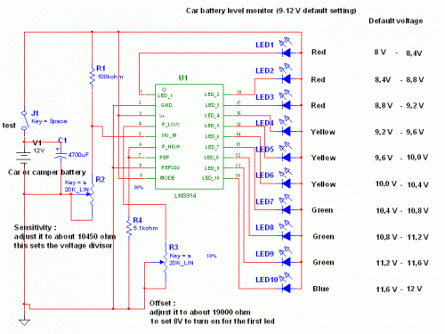
This circuit uses the popular and easy to find LM3914 IC. This IC is very simple to drive, needs no voltage regulators (it has a built in voltage regulator) and can be powered from almost every source. This circuit is very easy to explain: When the test button is pressed, the Car battery voltage is feed into a high impedance voltage divider. His purpose is to divide 12V to 1,25V (or lower values to lower values).

This solution is better than letting the internal voltage regulator set the 12V sample voltage to be feed into the internal voltage divider simply because it cannot regulate 12V when the voltage drops lower (linear regulators only step down). Simply wiring with no adjust, the regulator provides stable 1,25V which is fed into the precision internal resistor cascade to generate sample voltages for the internal comparators. Anyway the default setting let you to measure voltages between 8 and 12V but you can measure even from 0V to 12V setting the offset trimmer to 0 (but i think that under 9 volt your car would not start).

Circuit Project: Simple but reliable car battery tester

There is a smoothing capacitor (4700uF 16V) it is used to adsorb EMF noise produced from the ignition coil if you are measuring the battery during the engine working. Diesel engines would not need it, but I'm not sure. If you like more a point graph rather than a bar graph simply disconnect pin 9 on the IC (MODE) from power. The calculations are simple (default)
For the first comparator the voltage is : 0,833 V corresponding to 8 V
* * * * * voltage is : 0,875 V corresponding to 8,4 V
for the last comparator the voltage is : 1,25 V corresponding to 12 V
Have fun, learn and don't let you car battery discharge... ;-)
author: Jonathan Filippi
e-mail: jonathan.filippi@virgilio.it
Continue[...]

Solar-Powered High Efficiency Charger

This is a simple NiCd battery charger powered by solar cells. A solar cell panel or an array of solar cells can charge a battery at more than 80 % efficiency provided the available voltage exceeds the ‘fully charged’ battery voltage by the drop across one diode, which is simply inserted between the solar cell array and the battery. Adding a step-down regulator enables a solar cell array to charge battery packs with various terminal voltages at optimum rates and with efficiencies approaching those of the regulator itself. However, the IC must then operate in an unorthodox fashion (a.k.a. ‘Elektor mode’) regulating the flow of charge current in such a way that the solar array output voltage remains near the level required for peak power transfer. Here, the MAX639 regulates its input voltage instead of its output voltage as is more customary (but less interesting).

Circuit diagram:

Solar-Powered High Efficiency Charger Circuit Diagram

The input voltage is supplied by twelve amorphous solar cells with a minimum surface area of 100 cm2. Returning to the circuit, potential divider R2/R3 disables the internal regulating loop by holding the V-FB (voltage feedback) terminal low, while divider R1/R2+R3 enables LBI (low battery input) to sense a decrease in the solar array output voltage. The resulting deviation from the solar cells’ peak output power causes LBO (low battery output) to pull SHDN (shutdown) low and consequently disable the chip. LBI then senses a rising input voltage, LBO goes high and the pulsating control maintains maximum power transfer to the NiCd cells.

Current limiting inside the MAX639 creates a ‘ceiling’ of 200 mA for I out. Up to five NiCd cells may be connected in series to the charger output. When ‘on’ the regulator chip passes current from pin 6 to pin 5 through an internal switch representing a resistance of less than 1 ohm. Benefiting from the regulator’s low quiescent current (10 microamps typical) and high efficiency (85 %), the circuit can deliver four times more power than the single-diode configuration usually found in simple solar chargers. Coil L1 is a 100-µH suppressor choke rated for 600 mA.
Author: D. Prabakaran - Copyright: Elektor July-August 2004
Continue[...]

Sunday, September 30, 2012

Remote-Controlled Fan Regulator

Using this circuit, you can change the speed of the fan from your couch or bed. Infrared receiver module TSOP1738 is used to receive the infrared signal transmitted by remote control. The circuit is powered by regulated 9V. The AC mains is stepped down by transformer X1 to deliver a secondary output of 12V-0-12V. The transformer output is rectified by full-wave rectifier comprising diodes D1 and D2, filtered by capacitor C9 and regulated by 7809 regulator to provide 9V regulated output. Any button on the remote can be used for controlling the speed of the fan. Pulses from the IR receiver module are applied as a trigger signal to timer NE555 (IC1) via LED1 and resistor R4.
Circuit Diagram :
Remote-Controlled Fan Regulator Circuit Diagram
IC1 is wired as a monostable multivibrator to delay the clock given to decade counter-cum-driver IC CD4017 (IC2).Out of the ten outputs of decade counter IC2 (Q0 through Q9), only five (Q0 through Q4) are used to control the fan. Q5 output is not used, while Q6 output is used to reset the counter. Another NE555 timer (IC3) is also wired as a monostable multivibrator. Combination of one of the resistors R5 through R9 and capacitor C5 controls the pulse width.  The output from IC CD4017 (IC2) is applied to resistors R5 through R9. If Q0 is high capacitor C5 is charged through resistor R5, if Q1 is high capacitor C5 is charged through resistor R6, and so on.
Optocoupler MCT2E (IC5) is wired as a zero-crossing detector that supplies trigger pulses to monostable multivibrator IC3 during zero crossing. Opto-isolator MOC3021 (IC4) drives triac BT136. Resistor R13 (47-ohm) and capacitor C7 (0.01µF) combination is used as snubber network for triac1 (BT136). As the width of the pulse decreases, firing angle of the triac increases and speed of the fan also increases. Thus the speed of the fan increases when we press any button on the remote control. Assemble the circuit on a general-purpose PCB and house it in a small case such that the infrared sensor can easily receive the signal from the remote transmitter.
Continue[...]

Storage Battery Exerciser

A motorcycle or boat battery that is not needed over the winter is usually charged before being put away for the winter, after which it remains standing unused for months on end. As a result, it accumulates deposits of lead sludge, which can result in reduced capacity or even complete failure of the battery. If you don’t keep active, you rust! To avoid this, it’s necessary to keep the battery active even during the winter. This circuit does such a good job of exercising the battery that it doesn’t have to be recharged during the winter. It only has to be fully charged again in the spring before being used again. IC1.A is an astable multivibrator with an asymmetric duty cycle. The output is High for around 0.6 s and Low for around 40 s. IC1.B is wired as a comparator that constantly monitors the battery voltage. Its threshold voltage is set to 11.0 V using the trimpot.

Circuit diagram:
Storage Battery Exerciser Circuit Diagram

As soon as the battery voltage drops below this value, the comparator goes Low and D6 is cut off, allowing the second astable multivibrator IC1.C to oscillate at approximately 1.2 Hz. LED D7 then blinks to indicate that the battery must be charged. As long as the battery voltage is greater than 11 V, IC1.B is High. IC1.A is Low most of the time, and in this state D4 conducts and the inverting input of IC1.D is Low. This means that IC1.D is High most of the time, with T1 cut off. T1 only conducts during the 0.6-s intervals when IC1.A is High. In this state it allows current to pass through the lamp (12 V / 3 W), which forms the actual load for the battery. After this, darkness prevails again for 40 s. The average current consumption is approximately 5 mA. At this rate, a relatively new 40-Ah battery will take around one year to become fully discharged. However, this can vary depending on the condition of the battery, and it may be necessary to ‘top up’ the battery once during the winter.
Author: Ludwig Libertin - Copyright: Elektor Electronics
Continue[...]

Sunday, September 16, 2012

Solar Battery Protector Prevents excessive Discharge

This circuit prevents the battery in a solar lighting system from being excessively discharged. It's for small systems with less than 100W of lighting, such as several fluorescent lights, although with a higher rated Mosfet at the output, it could switch larger loads. The circuit has two comparators based on an LM393 dual op amp. One monitors the ambient light so that lamps cannot be turned on during the day. The second monitors the battery voltage, to prevent it from being excessively discharged. IC1b monitors the ambient light by virtue of the light dependent resistor connected to its non-inverting input. When exposed to light, the resistance of the LDR is low and so the output at pin 7 is low.

Circuit diagram:
Solar battery protector prevents excessive discharge circuit schematic
Solar Battery Protector Circuit Diagram

IC1a monitors the battery voltage via a voltage divider connected to its non-inverting input. Its inverting input is connected to a reference voltage provided by ZD1. Trimpot VR1 is set so that when the battery is charged, the output at pin 1 is high and so Mosfet Q1 turns on to operate the lights. The two comparator outputs are connected together in OR gate fashion, which is permissible because they are open-collector outputs. Therefore, if either comparator output is low (ie, the internal output transistor is on) then the Mosfet (Q1) is prevented from turning on. In practice, VR1 would be set to turn off the Mosfet if the battery voltage falls below 12V. The suggested LDR is a NORP12, a weather resistant type available from Farnell Electronic Components Pty Ltd.
Author: Michael Moore - Copyright: Silicon Chip Electronics
Continue[...]

10,000x With One Transistor

For a collector follower with emitter resistor, you’ll often find that the gain per stage is no more than 10 to 50 times. The gain increases when the emitter resistor is omitted. Unfortunately, the distortion also increases. With a ubiquitous transistor such as the BC547B, the gain of the transistor is roughly equal to 40 times the collector current (Ic), provided the collector current is less than a few milliamps. This value is in theory equal to the expression q/KT, where q is the charge of the electron, K is Boltzmann’s constant and T is the temperature in Kelvin.

For simplicity, and assuming room temperature, we round this value to 40. For a single stage amplifier circuit with grounded emitter it holds that the gain Uout /Uin (for AC voltage) is in theory equal to SRc. As we observed before, the slope S is about 40Ic. From this follows that the gain is approximately equal to 40I cRc. What does this mean? In the first instance this leads to a very practical rule of thumb: that gain of a grounded emitter circuit amounts to 40·I c·Rc, which is equal to 40 times the voltage across the collector resistor.

If Ub is, for example, equal to 12 V and the collector is set to 5V, then we know, irrespective of the values of the resistors that the gain will be about 40R(12–5) = 280. Notable is the fact that in this way the gain can be very high in theory, by selecting a high power supply voltage. Such a voltage could be obtained from an isolating transformer from the mains. An isolating transformer can be made by connecting the secondaries of two transformers together, which results in a galvanically isolated mains voltage.

Circuit diagram:

That means, that with a mains voltage of 240 Veff there will be about 340 V DC after rectification and filtering. If in the amplifier circuit the power supply voltage is now 340 V and the collector voltage is 2 V, then the gain is in theory equal to 40 x (340–2). This is more than 13,500 times! However, there are a few drawbacks in practice. This is related to the output characteristic of the transistor. In practice, it turns out that the transistor does actually have an output resistor between collector and emitter.

This output resistance exists as a transistor parameter and is called ‘hoe’. In normal designs this parameter is of no consequence because it has no noticeable effect if the collector resistor is not large. When powering the amplifier from 340 V and setting the collector current to 1 mA, the collector resistor will have a value of 338 k. Whether the ‘hoe’-parameter has any influence depends in the type of transistor. We also note that with such high gains, the base-collector capacitance in particular will start to play a role.

As a consequence the input frequency may not be too high. For a higher bandwidth we will have to use a transistor with small Cbc, such as a BF494 or perhaps even an SHF transistor such as a BFR91A. We will have to adjust the value of the base resistor to the new hfe. The author has carried out measurements with a BC547B at a power supply voltage of 30 V. A value of 2 V was chosen for the collector voltage. Measurements confirm the rule of thumb. The gain was more than 1,000 times and the effects of ‘hoe’ and the base-collector capacitance were not noticeable because of the now much smaller collector resistor.
Author: Gert Baars
Copyright: Elektor Electronics
Continue[...]