Thursday, January 30, 2014
2 X 50W ICs amplifier with STK4191

The above is a stereo amplifier circuit based on IC STK4191 with 2 X 50Watt output power 8 ohm impedance. And besides that you can use some of the IC can also be applied in this series include the STK4101, 4111, 4121, 5131, 4141, 4151, 5161, 4171, 4181, and 4191. Required supply voltage from 12 Volt to 35 Volt DC.Part List :
R1 = 22K
R2 = 22K
R3 = 560R
R4 = 56K
R5 = 1K
R6 = 1K
R7 = 100R
R8 = 2K
R9 = 2K
R10 = 4.7R
R11 = 2K2
R12 = 2K2
R13 = 4.7R
R14 = 100R
R15 = 56K
R16 = 560R
C1 = 0.1uF
C2 = 0.1uF
C3 = 100uF
C4 = 100uF
C5 = 100uF
C6 = 0.1uF
C7 = 47uF
C8 = 47uF
C9 = 0.1uF
C10 = 100uF
C11 = 100uF
U1 = STK4191
Tuesday, January 28, 2014
Tips for caring power supply units
 Power Supply on a computer is an energy source that drives the computer you. With power supply, hardware on the computer is given "power" to can work in accordance with their respective functions Power Supply on a computer to work as a flow modifier (Adapter) from AC current into DC.
1. Make sure you buy the power supply to suit your computer needs. Buy power supply that is guaranteed quality.
2. Make sure when you install a power supply on your computer already in the correct position. Make a tightening of the socket-outlet power supply to the motherboard, hard drive, CDRom, etc.. If you do the installation is not correct it will be fatal and can be a fire or a short-circuit will occur on your hardware.
3. Check your power supply voltages in the BIOS Hardware Monitor or Hardware Management. Is it permissible range qualified. If it does not fit will usually be marked with red writing.
4. Check the condition of the fan at any time at least 3 months. Or, when you have a problem on your computer such as Hang, Restart and Total death. Clean the fan if necessary and give a lubricant (contact cleaner) in as a fan.
5. Do not put your CPU is too close (mepet) with the wall. Because it would cause air circulation fan should be running with the operation will be disrupted.
Monday, January 27, 2014
16W Bridge Amplifier using LM383

This is an old amplifier, LM383 is discontinued, so this LM383 ability be difficult to find. You can use ECG1232, TDA2002 or TDA2003 as the alter for LM383. Take a agenda that a heatsink bowl is appropriate to abstain overheating on the ICs.
Sunday, January 26, 2014
Multiplexer with TTL IC 74251

C | B | A | G | Y | W |
X | X | X | 1 | Z | Z |
0 | 0 | 0 | 0 | D0 | D0’ |
0 | 0 | 1 | 0 | D1 | D1’ |
0 | 1 | 0 | 0 | D2 | D2’ |
0 | 1 | 1 | 0 | D3 | D3’ |
1 | 0 | 0 | 0 | D4 | D4’ |
1 | 0 | 1 | 0 | D5 | D5’ |
1 | 1 | 0 | 0 | D6 | D6’ |
1 | 1 | 1 | 0 | D7 | D7’ |
Z = High impedance (off) | |||||
D0,D1…D7 = Representing the output of the input lines D | |||||
Saturday, January 25, 2014
Elco tester circuit
 |
| Elco tester circuit |
- Make sure the position of the switch (SW1) on the discharging position (position A).
- Connect / elco pairs that will be tested, then empty the contents briefly elco by pressing SW2 (approximately 1 to 3 seconds).
- Position the switch in the charging position (position B), the LED will light with a certain time (depending on the value elco). Hold in position B until the LED is not lit (elco is full).
- When the LED is not lit, immediately moved to the position of discharging position (A), the LED will light with a certain time (depending on the value elco tested). Hold in position A until the LED does not turn on again (fill elco is empty).
- The conclusion is quite simple, the larger the size elco, the longer the charging time and dischargingnya (old LED lights up). To calibrate it, readers can use the benchmark elco 10000uF size that can be justified. Only by logic alone writers think readers have understood.
Good luck and commanded me, the value of its components should not be deleted, do not be wrapped up neatly, keep the same cast in epoxy / cement.
Friday, January 24, 2014
Digital Bike Tachometer Circuit

Thursday, January 23, 2014
Radio remote controls for toy cars
")
 |
| Radio Control Transmitter Series |
At the start chopping, all the output of IC 14 024 enumerators in kedaan 0 , after chopping 8 Q4 output pulse (pin 6) will be a 1, after counting 16 pulses output Q5 (pin 5) to 1 , after chopping 32 Q6 output pulse (pin 4) to 1 , after counting 64 pulses output Q7 (pin 3) to 1.
Output over-output voltage used to control foot 9 U2C through diode D1 and D2, during one of the output is still worth 0 then the clock generator U2B still working, this will continue until the cathode D1 D2 dankatode be 1 so that the foot 9 U2C be a 1 as well. This situation will result in the output feet 3 U2A to 1 , which stop the clock generator U2B and resets the enumerator 14 024 danberhenti already shipping 27 145 MHz pulse frequency.
To generate the lag time for receiver circuit has enough time carrying out orders, used a series of Q2 9014, resistor R7 and capacitor C10. The amount of delay time is determined by the value of R7 and C10. Switch to send command forward / backward and to send commands left / right are two separate switches. Each switch has 3 positions, the center position means that the scalar does not send commands.
 |
| Radio Control Receiver series |
How it works Receiver
Transistor Q2 follows perlangkapannya forming circuit to convert the radio frequency pulses received from the transmitter into the box pulses that can be accepted as a digital signal by the CMOS IC. Digital signal will be received as the clock had to be chopped by chopper 14 024 IC (U2). Output 14 024 will be in accordance with the number of pulses sent by the transmitter, forward command and left (which is used as an example in the discussion of the transmitter) is the pulse number of 24, the results of counting these pulses cause the output to be 14 024 Q4 = 1 , Q5 = 1, Q6 = 0 and Q7 = 0.
Digital signal received in addition be used as a clock IC 14 024 enumerators U2 discussed above, used also to drive the 3 pieces of the time delay circuit to generate pulses which controls the circuit work.
Toll regulator will first appear after delivery frequency pulse stopped because the lag time between sending the code, this pulse serves to record the count results to the U3 14 024 14 042 (D Flip Flop), making the final conditions of 14 024 will be retained to control the motor. After the results were recorded to 14 024 14 042, 14 042 enumerator is reset by the second pulse, after the lag time for 14,042 enumerators can count start from 0 again.
The circuit formed by transistors Q3, Q4, Q7, Q8, Q9 and Q10 named as H Bridge circuit, this circuit is very reliable to drive DC motors. With this series of DC motor can be rotated to the right-to-left or stop motion. The main requirement of the use of this circuit is the base voltage of Q7 and Q10 base voltage must be opposed, for example base Q7 = 1 and the base of Q10 = 0 the motor rotates to the left, the base of Q7 = 0 and the base of Q10 = 1 the motor will spin to the right, the base Q7 = 0 and the base Q10 = 0 motor stop motion, but it should not happen, the base Q7 = 1 and the base of Q10 = 1.
Similarly, Q5, Q6, Q11, Q12, Q13 and Q14 form a H Bridge. H Bridge to the left in Figure 2 is used to control motors that adjust the cars moving left / right, while the H Bridge right part is used to control motors that regulate movement forward / backward cars. The relationship between outpur enumerator 14 042 and 14 024 Input D Flip Flop is structured so that the signal is fed to each H Bridge can not be all 1 simultaneously.
Wire to the transformer can wear a wire in the unloading of these Koker, carefully open coil of wire that already exist within the Koker because the wire is smooth and quite easy to break.
Step 1: Roll away from the feet of wire fed into the number 5 ft 4 in the direction h (CW) as much as 3 rolls right in level 1 (point level above the lowest point)
Step 2: Wind the wire from leg 1 to leg 2 in a clockwise direction as much as 4 rolls right on level 2.
Step 3: Continue the roll (from step 2) clockwise a quarter roll to as much as 3 feet 3 at level three. (Can be determined exactly a quarter of the roll, because kokernya have a path cut into 4).
Making coil L1
Making coil L2
Wednesday, January 22, 2014
Digital Clock with Timer and Solar Panel Regulator
 |
| Basic Clock Circuit Diagram |
The basic clock circuit (top schematic below) is similar to the binary clock (on another page) and uses 7 ICs to produce the 20 digital bits for 12 hour time, plus AM and PM. A standard watch crystal oscillator (32,768) is used as the time base and is divided down to 1/2 half second by the 4020 binary counter. One half of a 4013 data latch is used to divide the 1/2 second signal by 2 and produce a one second pulse that drives the seconds counter (74HC390 colored purple). The minutes are advanced by decoding 60 seconds (40 + 20) and then resetting the seconds counter to 0 and at the same time advancing the minutes counter. The same procedure is used to advance the hours. The second half of the 4013 latch is used to indicate AM or PM and is toggled by decoding 13 hours and resetting the hours to 0 and then advancing the hours to "one".
 |
| Clock Display Circuit Diagram |
The clock display circuit is shown in the second drawing below and uses 6 more ICs to decode the binary data and drive four seven segment LED displays. The 10s of hours digit is driven with a single 3904 transistor. Two multiplexer circuits (4053) are used to manually select either minutes or seconds for the right two display digits. The two switches shown between the 4053s and below the left 4053 are both part of one DPDT switch which selects either seconds or minutes for the 1X and 10X digits. This switch is shown in the seconds position and the hours digits are blanked with a low signal on pin 4 of the 4511.
The display can also be toggled on and off (totally blank) using a set/reset latch made from a couple 74HC00 NAND gates. A momentary DPDT switch is used to control the latch and toggle the display on or off. The second pole of this switch is used on the upper drawing (connected to the run/stop switch) to set the hours and minutes. Thus this same switch performs both functions of blanking the display and setting the time. The run/stop switch is shown in the normal running mode and supplies a low signal to a NAND gate which prevents accidental setting the time while the clock is running.
 |
| Clock Timer Circuit Diagram |
The run/stop switch also turns on the display (through the diode D2) when in the stop position. The procedure for setting the clock would be to set the (run/stop) switch the stop position and the (seconds/minutes) switch to the minutes position. Then toggle the momentary switch to set minutes and hours of the current time plus one minute. The clock can then be started with the run/stop switch at precisely the right time (+/- 0.5 seconds).
 |
| Voltage Regulator (13.6 volts) |
The voltage regulator in the lower drawing maintains the battery at 13.6 volts and also supplies the clock and timer circuits with 4.3 volts. The charge LED indicator only comes on when the regulator is supplying max charge to the battery. When the battery voltage reaches 13.6 the regulator reduces the current to whatever is necessary to maintain the voltage and the charge indicator will turn off. The unit I built also included a battery condition indicator (voltmeter using 4 LEDs) to indicate the battery condition so that a failure of the regulator would be indicated by the charge indicator LED turned off and less than 4 LEDs lit on the voltmeter.
Tuesday, January 21, 2014
Touch Switch using NE555
This circuit uses 2 pieces of metal plate media as touch, MP1 (Metal Plate 1) and MP2 (Metal Plate 2). Touch switch circuit is equipped with a visual LED indicator for relay status (load active). To enable (Relay ON) can be done by touching the surface of MP1 and to turn it off by touching the surface of the MP2. MP1 and MP2 in touch this switch can use a small piece of copper (diameter 5mm) was enough.
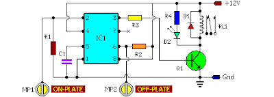
Component List 555 touch Switch
R1 = 3.3M
R2 = 3.3M
R3 = 10K
R4 = 1K
C1 = 10nF-63V
D1 = 1N4007
D2 = Red LED
Q1 = BC547
IC1 = NE555
RL1 = 12V Relay
Monday, January 20, 2014
Electronic Thermostat and Relay
Electronic Thermostat and Relay Circuit Diagram

In operation, the series resistor is adjusted so that the relay just toggles off at the desired temperature. A three degree drop in temperature should cause the relay to toggle back on and remain on until the temperature again rises to the preset level. The relay action can be reversed so it toggles off at the lower end of the range by reversing the locations of the 5K potentiometer and thermistor. The 5.1 volt zener diode regulates the circuit voltage so that small changes in the 12 volt supply will not effect operation. The voltage across the thermistor should be half the supply or about 2.6 volts when the temperature is within the 3 degree range set by the potentiometer. Most any thermistor can be used, but the resistance should be above 1K ohm at the temperature of interest. The series resistor selected should be about twice the resistance of the thermistor so the adjustment ends up near the center of the control.
Sunday, January 19, 2014
Booster BLW 60

Saturday, January 18, 2014
4 5 Mhz Notch Filter Schematic
4.5 Mhz Notch Filter Schematic

Friday, January 17, 2014
Differential amplifier circuit
 |
| Differential amplifier |
Thursday, January 16, 2014
2 X 50W ICs amplifier with STK4191
The above is a stereo amplifier circuit based on IC STK4191 with 2 X 50Watt output power 8 ohm impedance. And besides that you can use some of the IC can also be applied in this series include the STK4101, 4111, 4121, 5131, 4141, 4151, 5161, 4171, 4181, and 4191. Required supply voltage from 12 Volt to 35 Volt DC.Part List :
R1 = 22K
R2 = 22K
R3 = 560R
R4 = 56K
R5 = 1K
R6 = 1K
R7 = 100R
R8 = 2K
R9 = 2K
R10 = 4.7R
R11 = 2K2
R12 = 2K2
R13 = 4.7R
R14 = 100R
R15 = 56K
R16 = 560R
C1 = 0.1uF
C2 = 0.1uF
C3 = 100uF
C4 = 100uF
C5 = 100uF
C6 = 0.1uF
C7 = 47uF
C8 = 47uF
C9 = 0.1uF
C10 = 100uF
C11 = 100uF
U1 = STK4191
Wednesday, January 15, 2014
14 V battery charger circuit and troubleshooting
This circuit is also use operational amplifier IC LM324 to drive the VN64GA with the error signal and to control output voltage. This output voltage is pulsating DC , which is quite satisfactory for battery charging. This circuit also can be converted to the system regulated DC supply.
You do this by increased C2 and anoother electrolytic capacitor is added across the load. The respon time is very fast, determined by the op amp.
Schematic and troubleshooting below :

- AC cable disconnected
- Transformer is damaged or leaking.
- Broken or leaky diode.
- Installation of inverted foot elco.
- Instrallation of the components of the upside , particularly on the transistor , examine the placement of the feet emitter , collector and base.
- IC damaged.
- Soldering is less sticky.
- Line PCB damaged.
Tuesday, January 14, 2014
SMS Remote controller circuit
Series AVR ATTiny To SMS Remote Controller
 |
| SMS Remote controller circuit Click to view larger. |
AVR circuit this part ATTiny To SMS Remote Controller
- 4 Relay for ON / OFF electronic devices
- 8 input lines for reading in a normal switching
- LED indicators signal operator
- SMS command with password, so only the owner can operate
Monday, January 13, 2014
Schematic Audio Amplifier with IC AN5260

Sunday, January 12, 2014
1000W Mosfet Power Inverter
 |
| 1000W Mosfet Power Inverter |
Saturday, January 11, 2014
Control Relay Circuit with 9 Second
Friday, January 10, 2014
Audio Stereo Channel Selector Circuit
 Audio Stereo Channel Selector Circuit
This circuit has accouterment for abutting stereo outputs from four altered sources/channels as inputs and alone one of them is selected/connected to the achievement at any one time.
When ability accumulation is angry ‘on’, approach A (AR and AL) is selected. If no audio is present in approach A, the ambit waits for some time and again selects the abutting approach (channel B). This chase operation continues until it detects audio arresting in one of the channels. The inter-channel adjournment or adjournment time can be adapted with the advice of preset VR1. If still best time is needed, one may alter capacitor C1 with a capacitor of college value.
Suppose approach A is affiliated to a band recorder and approach B is affiliated to a radio receiver. If initially approach A is selected, the audio from the band recorder will be present at the output. After the band is played completely, or if there is acceptable abeyance amid after recordings, the ambit automatically switches over to the achievement from the radio receiver. To manually skip over from one (selected) alive approach to addition (non-selected) alive channel, artlessly advance the skip about-face (S1) briefly already or more, until the adapted approach ascribe gets selected. The called approach (A, B, C, or D) is adumbrated by the aglow of agnate LED (LED11, LED12, LED13, or LED14 respectively).
IC CD4066 contains four alternation switches. These switches are affiliated to four abstracted channels. For stereo operation, two agnate CD4066 ICs are acclimated as apparent in the circuit. These alternation switches are controlled by IC CD4017 outputs. CD4017 is a 10-bit arena adverse IC. Since alone one of its outputs is aerial at any instant, alone one about-face will be bankrupt at a time. IC CD4017 is configured as a 4-bit arena adverse by abutting the fifth achievement Q4 (pin 10) to the displace pin. Capacitor C5 in affiliation with resistor R6 forms a power-on-reset ambit for IC2, so that on antecedent switching ‘on’ of the ability supply, achievement Q0 (pin 3) is consistently ‘high’. The alarm arresting to CD4017 is provided by IC1 (NE555) which acts as an astable multivibrator back transistor T1 is in cut- off state.
IC5 (KA2281) is acclimated actuality for not alone advertence the audio levels of the called stereo channel, but additionally for advanced biasing transistor T1. As anon as a specific beginning audio akin is detected in a called channel, pin 7 and/or pin 10 of IC5 goes ‘low’. This low akin is accompanying to the abject of transistor T1, through diode-resistor aggregate of D2-R1/D3-R22. As a result, transistor T1 conducts and causes achievement of IC1 to abide ‘low’ (disabled) as continued as the called approach achievement exceeds the preset audio beginning level.
Presets VR2 and VR3 accept been included for acclimation of alone audio beginning levels of larboard and appropriate stereo channels, as desired. Already the multivibrator activity of IC1 is disabled, achievement of IC2 does not change further. Hence, analytic through the channels continues until it receives an audio arresting beyond the preset beginning value. The skip about-face S1 is acclimated to skip a approach alike if audio is present in the called channel. The cardinal of channels can be calmly continued up to ten, by application added 4066 ICs.
Thursday, January 9, 2014
Electronic Cricket Match Game
With the shown values of these components very fast output pulses are generated from the Astable. Output from IC1 passes into the input of IC2 which is the popular Johnson Decade counter CD4017. It has 10 outputs. Of these 8 outputs are used. Output 9 ( pin9) is tied to the reset pin 15 to repeat the cycle. When the input pin 14 of IC2 gets low to high pluses, its output turns high one by one. Resistor R3 keeps the input of IC2 low in stand by state to avoid false indications.
Electronic Cricket Circuit diagram:

When the Push Switch S1 is pressed momentarily, the Astable operates and all the LEDs run very fast sequentially. When S1 is released, any one of the LED stands lit which indicates the status of the match. For example, if LED D7 remains lit, it indicates Sixer and if LED 8 remains lit, it indicates Catch out. Label each LED for its status as shown in the diagram. Pressing of S1 simulates Bowling and Running LEDs indicates running of Batsman.
12 Volt to 32 Volt CT converter DC to DC

Kit converter is also equipped with inputs "SEND" to activate the circuit and also send this interchangeable inputs is connected to the Tape / cd / dvd player of your car. And input "send" is if the non-connected with an output of "send" player car you then connect it to +12 hrs on v from the battery / batteries The series is already in the test kit and has been functioning normally.