Saturday, October 25, 2014

Invisible Broken Wire Detector

Portable loads such as video cameras, halogen flood lights, electrical irons, hand drillers, grinders, and cutters are powered by connecting long 2- or 3-core cables to the mains plug. Due to prolonged usage, the power cord wires are subjected to mechanical strain and stress, which can lead to internal snapping of wires at any point. In such a case most people go for replacing the core/cable, as finding the exact location of a broken wire is difficult.

In 3-core cables, it appears almost impossible to detect a broken wire and the point of break without physically disturbing all the three wires that are concealed in a PVC jacket. The circuit presented here can easily and quickly detect a broken/faulty wire and its breakage point in 1-core, 2-core, and 3-core cables without physically disturbing wires. It is built using hex inverter CMOS CD4069.

Gates N3 and N4 are used as a pulse generator that oscillates at around 1000 Hz in audio range. The frequency is determined by timing components comprising resistors R3 and R4, and capacitor C1. Gates N1 and N2 are used to sense the presence of 230V AC field around the live wire and buffer weak AC voltage picked from the test probe. The voltage at output pin 10 of gate N2 can enable or inhibit the oscillator circuit.

When the test probe is away from any high-voltage AC field, output pin 10 of gate N2 remains low. As a result, diode D3 conducts and inhibits the oscillator circuit from oscillating. Simultaneously, the output of gate N3 at pin 6 goes ‘low’ to cut off transistor T1. As a result, LED1 goes off. When the test probe is moved closer to 230V AC, 50Hz mains live wire, during every positive half-cycle, output pin 10 of gate N2 goes high.

Thus during every positive half-cycle of the mains frequency, the oscillator circuit is allowed to oscillate at around 1 kHz, making red LED (LED1) to blink. (Due to the persistence of vision, the LED appears to be glowing continuously.) This type of blinking reduces consumption of the current from button cells used for power supply. A 3V DC supply is sufficient for powering the whole circuit.

Circuit diagram:
invisible broken wire detector circuit schematic
Invisible Broken Wire Detector Circuit Diagram

AG13 or LR44 type button cells, which are also used inside laser pointers or in LED-based continuity testers, can be used for the circuit. The circuit consumes 3 mA during the sensing of AC mains voltage. For audio-visual indication, one may use a small buzzer (usually built inside quartz alarm time pieces) in parallel with one small (3mm) LCD in place of LED1 and resistor R5. In such a case, the current consumption of the circuit will be around 7 mA.

Alternatively, one may use two 1.5V R6- or AA-type batteries. Using this gadget, one can also quickly detect fused small filament bulbs in serial loops powered by 230V AC mains.
The whole circuit can be accommodated in a small PVC pipe and used as a handy broken-wire detector. Before detecting broken faulty wires, take out any connected load and find out the faulty wire first by continuity method using any multimeter or continuity tester.

Then connect 230V AC mains live wire at one end of the faulty wire, leaving the other end free. Connect neutral terminal of the mains AC to the remaining wires at one end. However, if any of the remaining wires is also found to be faulty, then both ends of these wires are connected to neutral. For single-wire testing, connecting neutral only to the live wire at one end is sufficient to detect the breakage point.

In this circuit, a 5cm (2-inch) long, thick, single-strand wire is used as the test probe. To detect the breakage point, turn on switch S1 and slowly move the test probe closer to the faulty wire, beginning with the input point of the live wire and proceeding towards its other end. LED1 starts glowing during the presence of AC voltage in faulty wire. When the breakage point is reached, LED1 immediately extinguishes due to the non-availability of mains AC voltage.

The point where LED1 is turned off is the exact broken-wire point. While testing a broken 3-core rounded cable wire, bend the probe’s edge in the form of ‘J’ to increase its sensitivity and move the bent edge of the test probe closer over the cable. During testing avoid any strong electric field close to the circuit to avoid false detection.
 
Author: K. Udhaya Kumaran
Continue[...]

Transformer Less Power Supply Circuit Diagram

This clever design uses 4 diodes in a bridge to produce a fixed voltage power supply capable of supplying 35mA. All diodes (every type of diode) are zener diodes. They all break down at a particular voltage. The fact is, a power diode breaks down at 100v or 400v and its zener characteristic is not useful.  But if we put 2 zener diodes in a bridge with two ordinary power diodes, the bridge will break-down at the voltage of the zener. This is what we have done. If we use 18v zeners, the output will be 17v4.
When the incoming voltage is positive at the top, the left zener provides 18v limit (and the left power-diode produces a drop of 0.6v).  This allows the right zener to pass current just like a normal diode but the voltage available to it is just 18v.  The output of the right zener is 17v4. The same with the other half-cycle.  The current is limited by the value of the X2 capacitor and this is 7mA for each 100n when in full-wave (as per thiscircuit). We have 10 x 100n = 1u capacitance. Theoretically the circuit will supply 70mA but we found it will only deliver 35mA before the output drops. The capacitor should comply with X1 or X2 class. The 10R is a safety-fuse resistor.
Circuit diagram:
TransformerLess Power-Supply-Circuit-Diagram
TransformerLess Power Supply Circuit Diagram 
The problem with this power supply is the "live" nature of the negative rail. When the power supply is connected as shown, the negative rail is 0.7v above neutral. If the mains is reversed, the negative rail is 340v (peak) above neutral and this will kill you as the current will flow through the diode and be lethal. You need to touch the negative rail (or the positive rail) and any earthed device such as a toaster to get killed. The only solution is the project being powered must be totally enclosed in a box with no outputs. 
Continue[...]

Thursday, October 23, 2014

Arduino Based Capacitive Touch Screen

Arduino based projects are quite complicated and is no cake walk for beginners in this field. Interfacing a tablet with the microcontroller is a daunting task. Let see how its done here.


Hacks and Mods: Arduino Based Capacitive Touch Screen
 
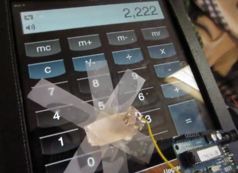
The primary focus should be on using the appropriate drivers for the tablet. This makes it a USB host. As seen in the video, light can be a medium of communication between the tablet and the microcontroller. A photo diode or photoresistor is what is needed here and this should be pressed against the screen.

Building a touch sensing capability can help in providing communication between the microcontroller and the tablet. Capacitive touch screens function by sensing the capacitance changes on the screen. In this case, a large conductive brass plate is used to simulate touch. The surface area of the conductor used here to simulate the touch sould be large.

Testing can be done by touching the scrren with a wire and holding the other end. This may not work. This is made to work by sticking a piece of aluminum foil on to the screen and connecting the free end to the pin that is available on the arduino. The video shows the working of the capacitive touch screen. The setup is quite fragile and a little more circuitry could improve its reliability. Thus the capacitive touch screen is done.
Continue[...]

Panasonic Microwave Oven Inverter HV Power Supply

Nearly all Panasonic microwave ovens now use an Inverter, and are always labelled with “Inverter” on
the front.

The High Voltage Power Supply Unit (HV PSU)
The HV PSU measures 165mm x 105mm x 60mm and weighs 650g.
 At left is the control daughter board. In front of that on the main board are the opto-isolators for the control and status signals brought out to the green connector. Back left is the rectified mains filter choke. The mains rectifier and switching transistors can just be seen on the heatsink behind the transformer. The mains filter capacitor is at right rear. The HV rectifiers and filters (doubler) are right front – white wires are the HV output from the transformer. The green wire is for grounding the HV +ve. The two lugs t right are for connecting HV -ve and heater to the magnetron. The winding thatcan be seen on the transformer is the primary and is made from 3mm finely stranded wire.

Here’s a view of the control end: 


This is the high voltage end:


The circuit for the HV PSU is below 

Notes about the circuit:
1. Apart from the block diagram, there is no information on the Inverter cont(o)rol circuit. The circuit itself is centred on one large, unmarked IC, so no help there.
2. The control and status signals seem to be a digital stream (2-3v suggestsa 5V data stream). They are opto-isolated because the majority of the circuit is at mains potential  (**BEWARE**). The part that isn’t is at 4kV (*** REALLY BEWARE ***)
3. The mains input side is monitored for both current and (under) voltage. No indication of what the control circuit does with this information.
4. The mains filter capacitor (C702) is very small – only 4uF. In a “normal” switching supply, there is usually 220 or 470 uF in this position.
5. Q701 that does all the hard work is a very heavy duty IGBT – a GT60N90 - 900V @ 60 A. Q702 forms some sort of flywheel circuit. This circuit from a Toshiba IGBT application note looks similar:
6. The HV side has a full-wave doubler rectifier and is marked 4kV @  300mA. Unlike the classic microwave oven transformers (where one side of the winding is grounded), this means that the secondary must be well insulated from ground on both sides. A simple reconfiguration of the rectifier (replace the caps with diodes) into a bridge circuit should yield 2kV @ 600mA (depending on the diode ratings)
7. The HV filter capacitors are only 8200 pF each, effectively giving 4100pF in the doubler. Considering that the inverter runs at about 30kHz, the reactance is equivalent to that  of a 5uF capacitor at 50Hz.
8. The positive side of the HV is grounded, so it’s a –4kV supply. Don’t simply swap the ground from the positive to the negative to get a +4kV supply, as the core of the transformer is also connected to this ground trace and will suddenly rise to 4kV above ground with disastrous and potentially fatal results. Instead, reverse the polarity of the rectifier diodes to get +4kV.


Source : By David Smith VK3HZ (vk3hz (*at*) wia.org.au)
Continue[...]

Line Following Robot Sensor

This Line Following Robot sensor or surface scanner for robots is a very simple, stamp-sized, short range (5-10mm) Infrared proximity detector wired around a standard reflective opto-sensor CNY70(IC1). In some disciplines, a line following robot or an electronic toy vehicle go along a predrawn black line on a white surface. In such devices, a surface scanner, pointed at the surface is used to align the right track.

IC1 contains an infrared LED and a phototransistor. The LED emit invisible infrared light on the track and the phototransistor works as a receiver. Usually, black colored surface reflects less light than white surface and more current will flow through the phototransistor when it is above a white surface. When a reflection is detected (IR light falls on the phototransistor) a current flows through R2 to ground which generates a voltage drop at the base of T1 to make it conduct. As a result, transistor T2 start conducting and the visual indicator LED(D1) lights up. Capacitor C2 works as a mini buffer.

Line Follower Robot Scanner Schematic

Circuit Project: Line Following Robot Sensor

After construction and installation, the scanner needs to be calibrated. Initially set P1 to its mechanical centre position and place the robot above the white portion of the track. Now slowly turn P1 to get a good response from D1. After this, fine tune P1 to reduce false detection caused by external light sources. Also ensure that the LED remains in off condition when the sensor module is on the blackarea. Repeat the process until the correct calibration is achieved.

The red color LED (D1) is only a visual indicator. You can add a suitable (5V) reed relay in parallel with D1-R4 wiring after suitable alterations to brake/stop/redirect the robot. Similarly, the High to low (H-L) transition at the collector of T2 can be used as a signal to control the logic blocks of the robot. Resistor R1 determines the operating current of the IRLED inside IC1. The sensing ability largely depends on the reflective properties of the markings on the track and the strength of the light output from IC1.
Continue[...]

Using LTC3601 3 3V DC Power Converter

This Dc power converter circuit is designed LTC3601 from Linear Technology and is capable to up to 1.5A output current at a 3.3V. The LTC3601 operating supply voltage range is from 4V to 15V making it suitable for a wide range of power supply applications. The operating frequency of the LTC3601 buck regulator is programmable from 800kHz to 4MHz with an external resistor enabling the use of small surface mount inductors.

 The LTC3601 buck regulator can operate in two modes: Burst Mode operation and forced continuous mode to allow the user to optimize output voltage ripple, noise, and light load efficiency for a given application.
Continue[...]

Friday, October 17, 2014

Single IC Dual tones Siren Circuits Diagram

Double-tone Police sound Circuits Diagram

This circuit is intended for children fun, and can be installed on bicycles, battery powered cars and motorcycles, but also on models and various games and toys. With SW1 positioned as shown in the circuit diagram, the typical dual-tone sound of Police or Fire-brigade cars is generated, by the oscillation of IC1A and IC1B gates. With SW1 set to the other position, the old siren sound increasing in frequency and then slowly decreasing is reproduced, by pushing on P1 that starts oscillation in IC1C and IC1D. 

The loudspeaker, driven by Q1, should be of reasonable dimensions and well encased, in order to obtain a more realistic and louder output. Tone and period of the sound oscillations can be varied by changing the values of C1, C2, C5, C6 and/or associated resistors. No power switch is required: leave SW1 in the low position (old-type siren) and the circuit consumption will be negligible.

Single -IC Dual-tones Siren Circuits Diagram


Parts:

R1,R3___470K   1/4W Resistors
R2______680K   1/4W Resistor
R4_______82K   1/4W Resistor
R5______330K   1/4W Resistor
R6_______10K   1/4W Resistor
R7_______33K   1/4W Resistor
R8________3M3  1/4W Resistor
 
C1,C5_____10µF  25V Electrolytic Capacitors
C2,C6_____10nF  63V Polyester Capacitors
C3_______100nF  63V Polyester Capacitor
C4_______100µF  25V Electrolytic Capacitor
 
D1-D3___1N4148  75V 150mA Diodes
 
IC1_____4093   Quad 2 input Schmitt NAND Gate IC
 
Q1______BC337   45V 800mA NPN Transistor
 
P1______SPST Pushbutton
 
SW1_____DPDT Switch
 
SPKR____8 Ohm Loudspeaker
 
B1______6V Battery (4 AA 1.5V Cells in series)
Continue[...]

iPod Controlled Sports Car

One of the most interesting things you can do with the iPod touch is using it as a remote control for other devices that is why some created remote control applications.

Hacks and Mods: IPod Controlled Sports Car
The entire device was rewired to allow the owner to start the car, open the doors and trunk, roll down the windows, control the radio, the car alarm and even the engine. The range of this is limited because the communication is through Bluetooth. What makes this car different from other remote controlled; it can be controlled via voice commands.

Hacks and Mods: IPod Controlled Sports Car

It is conceivable that an iPod touch could replace the fanciest of universal remotes and it is worth a try for all the hobbyists out there.
Continue[...]

Fog Lamp Sensor Circuit Diagram

For several years now, a rear fog lamp has been mandatory for trailers and caravans in order to improve visibility under foggy conditions.
Circuit diagram :
Fog Lamp Sensor-Circuit Diagram
Fog Lamp Sensor Circuit Diagram
When this fog lamp is switched on, the fog lamp of the pulling vehicle must be switched off to avoid irritating reflections. For this purpose, a mechanical switch is now built into the 13-way female connector in order to switch off the fog lamp of the pulling vehicle and switch on the fog lamp of the trailer or caravan. For anyone who uses a 7-way connector, this switching can also be implemented electronically with the aid of the circuit illustrated here.
Here a type P521 optocoupler detects whether the fog lamp of the caravan or trailer is connected. If the fog lamp is switched on in the car, a current flows through the caravan fog lamp via diodes D1 and D2. This causes the LED in the optocoupler to light up, with the result that the phototransistor conducts and energises the relay via transistor T1. The relay switches off the fog lamp of the car.
For anyone who’s not all thumbs, this small circuit can easily be built on a small piece of perforated circuit board and then fitted somewhere close to the rear lamp fitting of the pulling vehicle.
Continue[...]

Para saki the QRP Transceiver fact Diodes Circuit Diagram

This circuit is a dream of 40 years was conducted, a transceiver QRP (low power) done without transistors, IC or valves, its creator just used diodes. The receiver has little gain, but works well for strong signals via the audio amplifier which is very effective.I believe this transceiver is at least very curious, though precarious it sure works and shows that the electron has no limits.

Para-saki the QRP Transceiver fact Diodes Circuit Diagram


Parasaki the QRP Transceiver fact Diodes Circuit Diagram
Continue[...]

Simple Water Alarm Schematic

The LM1830 fluid detector IC from National Semiconduc tor is designed to be able to detect the presence of fluids using a probe. This chip requires a relatively high supply voltage and is not the most frugal power consumer. It is also quite specialised so unless you are buying in bulk the one-off price is not cheap. 

An alternative circuit show n her e uses a standard CMOS IC type 74HC14. It has the advantage of operating with a 3 V supply and consumes less than 1 µA when the alarm is not sounding, this makes it ideal for use with batteries. 

Water Alarm Schematic Circuit Diagram
Simple Water Alarm Schematic

The 74HC14 has six inverters with hysteresis on their input switching thresholds. A capacitor (C1) and a feedback resistor (R1) is all that’s necessary to make an inverter into a square wave signal generator. 

In the water alarm circuit the feedback resistor consists of R1 and the water sensor in series. R1 prevents any possibility of short-circuit between the inverter’s input and out-put. Resistor R2 defines the inverter’s input signal level when the sensor is not in water. Any open-circuit (floating) input can cause the inverter to oscillate and draw more current.The remaining inverters in the package (IC1.B to IC1.F) drive the piezo buzzer to produce an alarm signal. Capacitor C2 ensures that no DC current flows when the circuit is in monitoring mode (with the alarm silent) this helps reduce the supply current. 

A micro-switch can also be substituted for the water sensor to make the circuit a more general purpose alarm generator. link


Author: Roland Heimann - Copyright: Elektor
Continue[...]

USB 5V to 12V DC DC Step Up Converter by LT1618

This is a 5V to 12V DC-DC step-up (boost) converter circuitry that is especially ideal for the USB powered applications. First of all a USB port has two current supply modes. Before detecting the connected device, it supplies maximum 100mA to the load. After recognizing the device, it increases the output current up to 500mA. In this circuit, controller (LT1618) also provides two input current modes. 100mA and 500mA input modes can be selected by the user.

USB 5V to 12V DC-DC Step-Up Converter by LT1618
Output currents are limited due to the increased potential difference at the output. When the demand of the load increases, output voltage will start to decrease. For example, if the circuit operates in the 100 mA input mode, when the load is 35 mA, the output voltage will be kept at 12V. But if the load increases to 50 mA, output voltage will reduce to 8V to maintain the constant 100 mA input current.
Continue[...]

build a Low Cost Stereo Level Indicator

Usually, Low-Cost Stereo Level Indicator home stereo power amplifiers don’t have output level indicators. An output power level indicator can be added to each channel of these stereo power amplifiers. As low levels of the output power are not disturbing and damaging to the people, there is no need to add a preamplifier and low-level detector before IC LM3915. But you should know when the output power becomes considerably high.

Here we present a very simple, low-cost stereo-level indicator circuit for home power amplifiers with power rating of around 0.5W. The circuit is built around two LM3915 dot/bar display driver ICs (IC1 and IC2). LM3915 senses analogue voltage levels to drive ten LEDs, providing a logarithmic 3dB/step analogue display.

Stereo Level Indicator Circuit Diagram


The voltage levels below 1V are not important because these correspond to a low level of the audio signal. Similarly, input voltage levels above 30V correspond to too high levels of the output power, which are not applicable for home power amplifiers. So the voltage levels of our interest are 1V to 30V, which can be handled directly with LM3915. LM3915 needs no protection against ±35V inputs, which simplifies the circuit.

Most audio power amplifiers can drive 2-ohm to around 32-ohm loads. A load of several kilo-ohms will not change the conditions for the amplifier. CON1 is the input connector and CON2 output connector for the loudspeaker or headphone. Each channel has its own LM3915 and ten LEDs to indicate the power level. To indicate the different audio levels, select LEDs of three colours as per your liking. For example, you can have five green LEDs, three yellow LEDs and two red LEDs.

If appropriate signal generators and measuring equipment are not available, the level indicator can be calibrated based on personal observations. For example, the audio signal should be in the green LEDs zone when the signal is strong enough but not irritating, in the yellow zone when it is disturbing or starting to get distorted, and in the red zone when it is heavily distorted or too strong to listen to in the room.

Calibration can be done with the help of potentiometers VR1 and VR2, which are optional. Switches S1 and S2 let you select between two modes of LM3915 operation—the bar mode and the dot mode. These too can be removed or replaced with jumpers, if not required. When the switches are removed, leave pins 9 of IC1 and IC2 open.

The circuit works off regulated 12V. You can also power it through a 12V rechargeable battery.

Assemble the circuit on a general-purpose PCB and enclose in a suitable cabinet. Fix all the LEDs in two rows on the front side of the cabinet. Also affix the two terminals for input and output on rear side of the cabinet. 
link
Continue[...]

Small Circuit Multiband Radio Transmitter CW


Small Circuit Multiband Radio - Transmitter CW

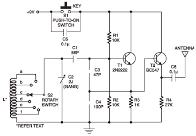
This is a Small Circuit Multiband Radio -Transmitter CW for who wants to learn more about radiofrequency, mainly operating principle from radios transceivers multiband, That circuit consists of a frequency oscillator RF, which is the main component us transmitters and radio receivers. 

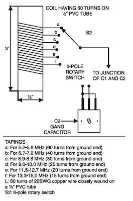
He oscillates for high frequency, he is called variable frequency oscillator or VFO, their frequency may vary of 5.2 MHz to 15 MHz, depending the coil chosen and signal can be received in the band shortwave by any receiver radio.In S1 is used a switch type bell, but can-if use a handler CW, these used by radio amateurs. How antenna should-if use a the type dipole from 1/4 wave.

Small Circuit Multiband Radio - Transmitter CW


Continue[...]

Thursday, January 30, 2014

2 X 50W ICs amplifier with STK4191

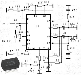
STK4191 amplifier schematics
The above is a stereo amplifier circuit based on IC STK4191 with 2 X 50Watt output power 8 ohm impedance. And besides that you can use some of the IC can also be applied in this series include the STK4101, 4111, 4121, 5131, 4141, 4151, 5161, 4171, 4181, and 4191. Required supply voltage from 12 Volt to 35 Volt DC.
Part List :
R1 = 22K
R2 = 22K
R3 = 560R
R4 = 56K
R5 = 1K
R6 = 1K
R7 = 100R
R8 =  2K
R9 = 2K
R10 = 4.7R
R11 = 2K2
R12 = 2K2
R13 = 4.7R
R14 = 100R
R15 = 56K
R16 = 560R
C1 = 0.1uF
C2 = 0.1uF
C3 = 100uF
C4 = 100uF
C5 = 100uF
C6 = 0.1uF
C7 = 47uF
C8 = 47uF
C9 = 0.1uF
C10 = 100uF
C11 = 100uF
U1 = STK4191
Continue[...]

Tuesday, January 28, 2014

Tips for caring power supply units

tips merawat komputerPower Supply on a computer is an energy source that drives the computer you. With power supply, hardware on the computer is given "power" to can work in accordance with their respective functions Power Supply on a computer to work as a flow modifier (Adapter) from AC current into DC. 

Power supply is working on 2 pieces of 5-volt DC voltage and 12 Volt. In a power supply, voltage 12 volt is usually characterized with a yellow cable, while the voltage is 5 Volt is marked with cable red.

PSU schematics

Tips to maintain power supply in order to remain durable

1. Make sure you buy the power supply to suit your computer needs. Buy power supply that is guaranteed quality.

2. Make sure when you install a power supply on your computer already in the correct position. Make a tightening of the socket-outlet power supply to the motherboard, hard drive, CDRom, etc.. If you do the installation is not correct it will be fatal and can be a fire or a short-circuit will occur on your hardware.

3. Check your power supply voltages in the BIOS Hardware Monitor or Hardware Management. Is it permissible range qualified. If it does not fit will usually be marked with red writing.

4. Check the condition of the fan at any time at least 3 months. Or, when you have a problem on your computer such as Hang, Restart and Total death. Clean the fan if necessary and give a lubricant (contact cleaner) in as a fan.

5. Do not put your CPU is too close (mepet) with the wall. Because it would cause air circulation fan should be running with the operation will be disrupted.
Continue[...]

Monday, January 27, 2014

16W Bridge Amplifier using LM383

16W Bridge Amplifier using LM383

The afterward diagram is 16W Bridge audio amplifier circuit. The ambit congenital based 2 pieces of ability IC LM383 in arch connection, so this amplifier is an arch amplifier.

This is an old amplifier, LM383 is discontinued, so this LM383 ability be difficult to find. You can use ECG1232, TDA2002 or TDA2003 as the alter for LM383. Take a agenda that a heatsink bowl is appropriate to abstain overheating on the ICs.

Continue[...]

Sunday, January 26, 2014

Multiplexer with TTL IC 74251

Actually you can not bother to design a multiplexer using logic gates because it has many special IC which functioned for a multiplexer.

One of the TTL ICs from the family that you can use to fulfill the function of a multiplexer is IC 74 251. At the IC there are 8 input channels and 3-bit selector and the other lane as a control reset and inverting output. As a note if you are using TTL ICs for your electronic circuit, the voltage supply that is allowed a maximum of 5 volts. So you can be more familiar with the workings of this multiplexer ic, IC74251 consider the truth table below:


C
B
A
G
Y
W
X
X
X
1
Z
Z
0
0
0
0
D0
D0’
0
0
1
0
D1
D1’
0
1
0
0
D2
D2’
0
1
1
0
D3
D3’
1
0
0
0
D4
D4’
1
0
1
0
D5
D5’
1
1
0
0
D6
D6’
1
1
1
0
D7
D7’
Z = High impedance (off)
D0,D1…D7 = Representing the output of the input lines D

Continue[...]

Saturday, January 25, 2014

Elco tester circuit

elco capastor tester
Elco testing small to use AVO meters. But to distinguish between the elco elco 20.000uF/50V 2200uF/50V size would be very difficult, perhaps this phenomenon that makes creative hands itch to make elco with two label values.


Scheme tool as follows, do not smile once, indeed simple. The cost to make it too cheap, not up to $ 1.

Elco tester circuit
Elco tester circuit

The workings of this tool based on the nature of the condenser, the condenser ability to store electrons / voltage. Since each condenser has the characteristic charging time and discharging time is different for each size and type dielektrika. Ideally, the larger size, the greater the time required for charging and discharging (charging and disposal charges).
How to use:

  • Make sure the position of the switch (SW1) on the discharging position (position A).
  • Connect / elco pairs that will be tested, then empty the contents briefly elco by pressing SW2 (approximately 1 to 3 seconds).
  • Position the switch in the charging position (position B), the LED will light with a certain time (depending on the value elco). Hold in position B until the LED is not lit (elco is full).
  • When the LED is not lit, immediately moved to the position of discharging position (A), the LED will light with a certain time (depending on the value elco tested). Hold in position A until the LED does not turn on again (fill elco is empty).
  • The conclusion is quite simple, the larger the size elco, the longer the charging time and dischargingnya (old LED lights up). To calibrate it, readers can use the benchmark elco 10000uF size that can be justified. Only by logic alone writers think readers have understood.
If it is the process of charging and discharging too quickly, the reader can change the value of R1, the greater the value the longer the charging process and discharging.

Good luck and commanded me, the value of its components should not be deleted, do not be wrapped up neatly, keep the same cast in epoxy / cement.
Continue[...]

Friday, January 24, 2014

Digital Bike Tachometer Circuit


This digital DIY tachometer for bikes uses two reed switches to get the speed information of the bicycle. The reed switches are installed near the rim of the wheel where permanent magnets pass by. The permanent magnets are attached to the wheelspokes and activate the reed switches everytime they pass by it. The speed is digitally displayed.

Electronic bicycle DIY tachometer circuit diagram
Digital Bike Tachometer

The tachometer circuit works according to this principle; the pulses created by the reed contacts are counted within a certain time interval. The resulting count is then displayed and represents the speed of the bike. Two 4026 ICs are used to count the pulses, decode the counter and control two 7-segment LED display. RS flip-flops U3 and U4 function as anti-bounce.

The pulses arrive at the counter’s input through gate U7. The measuring period is determined by monostable multivibrator U5/U6 and can be adjusted through potentiometer P1 so that the tacho can be calibrated. The circuit U1/U2 resets the counters.

Since batteries are used to power the circuit, it is not practical to support the continous display of speed information. This circuit is not continously active. The circuit is activated only after a button is pressed. At least three permanent magnets must be installed on the wheel. The circuit can be calibrated with the help of another precalibrated tachometer.
Continue[...]

Thursday, January 23, 2014

Radio remote controls for toy cars

Radio remote controls for toy cars (RC)
Playing cars that are controlled via radio signals is an interesting game. The much-loved toy cars children, plus a simple circuit will be the ideal toy car. This circuit families use traditional digital CMOS IC which requires very little electrical current, so it will not burden the original toy car performance.

In this system, radio signals are not transmitted continuously but only generated when the controller sends a command to the left / right or forward / backward, and even then only a radio-frequency discontinuous, so is sending pulses of radio wave frequency.

The number of pulses sent represent commands sent, GO command is represented with 8 pulses, is represented with 16 pulses LEFT, RIGHT DOWN 32 pulses and 64 pulses. Commands that can dikirimk is a combination of 2 orders once gus, which is a combination of command forward / backward and right / left, for example, could be sent forward orders and left once gus, in this case the number of pulses sent is 24, ie the sum of the forward command by 8 pulse and left the command of 16 pulses.

After a command is sent, the system stops sending commands in a certain time lag, the lag time it takes will be a series of recipients have sufficient time to fulfilling their orders well. Frequency pulses were visible on the right side of this.
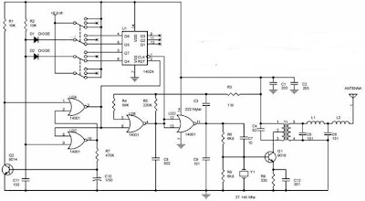


Radio Control Transmitter Series


How it works Transmitter
Radio signals generated by oscillator circuit formed by transistors Q1 9016, the working frequency of the oscillator is determined by the crystal Y1 is worth 27.145 MHz. A very critical part of this oscillator circuit is T1, L1 and L2, which specifically dealt with separately at the end of this article. Working from this oscillator is controlled by NOR gate U2D 14001, while the output gate (pin 3) is worth 1, the oscillator will work and transmit radio frequency 27.145 MHz, and at the output U2D value 0 the oscillator will stop working. U2D NOR gate receives the clock signal from NOR gate U2B. NOR Gate CMOS type with the aid of resistors R4 and R5 and capacitor C8 form a low frequency oscillator circuit for controlling the clock shaper of existing digital circuits. Work of this clock generator is controlled via the input leg 6, the circuit will generate the clock if this input berlevel 0 .

NOR gate U2A and U2C form a series of Latch (RS Flip Flop), because of the influence of the resistor R2 and capacitor C11 is fed to pin 9 in U2C, when the circuit gets power supply output U2C must be 1 and the output of U2A (leg number 3) becomes 0 . This situation resulted Marja U2b clock generator works evoke reset the clock and remove the state of the enumerator 14 024 IC (U1), so that U1 started chopping and 27.145 MHz oscillator circuit sending pulses for generating a clock frequency of work.

At the start chopping, all the output of IC 14 024 enumerators in kedaan 0 , after chopping 8 Q4 output pulse (pin 6) will be a 1, after counting 16 pulses output Q5 (pin 5) to 1 , after chopping 32 Q6 output pulse (pin 4) to 1 , after counting 64 pulses output Q7 (pin 3) to 1.

Output over-output voltage used to control foot 9 U2C through diode D1 and D2, during one of the output is still worth 0 then the clock generator U2B still working, this will continue until the cathode D1 D2 dankatode be 1 so that the foot 9 U2C be a 1 as well. This situation will result in the output feet 3 U2A to 1 , which stop the clock generator U2B and resets the enumerator 14 024 danberhenti already shipping 27 145 MHz pulse frequency.

To generate the lag time for receiver circuit has enough time carrying out orders, used a series of Q2 9014, resistor R7 and capacitor C10. The amount of delay time is determined by the value of R7 and C10. Switch to send command forward / backward and to send commands left / right are two separate switches. Each switch has 3 positions, the center position means that the scalar does not send commands.
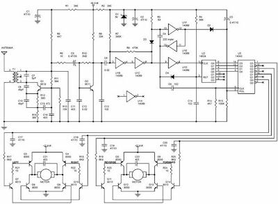


Radio Control Receiver series

How it works Receiver
Figure 2 is a picture that matched the car receiver circuit toy, serves to receive signals from the transmitter to control motor cars, so cars can move forward / backward and left / right. Transistor Q1 with the help of resistors, capacitors and T1 form as a series of radio signal receiver 27.145 MHz. T1 in this series exactly the same as T1 that is used in the transmitter circuit, means of manufacture are discussed below.

Transistor Q2 follows perlangkapannya forming circuit to convert the radio frequency pulses received from the transmitter into the box pulses that can be accepted as a digital signal by the CMOS IC. Digital signal will be received as the clock had to be chopped by chopper 14 024 IC (U2). Output 14 024 will be in accordance with the number of pulses sent by the transmitter, forward command and left (which is used as an example in the discussion of the transmitter) is the pulse number of 24, the results of counting these pulses cause the output to be 14 024 Q4 = 1 , Q5 = 1, Q6 = 0 and Q7 = 0.

Digital signal received in addition be used as a clock IC 14 024 enumerators U2 discussed above, used also to drive the 3 pieces of the time delay circuit to generate pulses which controls the circuit work.

Toll regulator will first appear after delivery frequency pulse stopped because the lag time between sending the code, this pulse serves to record the count results to the U3 14 024 14 042 (D Flip Flop), making the final conditions of 14 024 will be retained to control the motor. After the results were recorded to 14 024 14 042, 14 042 enumerator is reset by the second pulse, after the lag time for 14,042 enumerators can count start from 0 again.

The circuit formed by transistors Q3, Q4, Q7, Q8, Q9 and Q10 named as H Bridge circuit, this circuit is very reliable to drive DC motors. With this series of DC motor can be rotated to the right-to-left or stop motion. The main requirement of the use of this circuit is the base voltage of Q7 and Q10 base voltage must be opposed, for example base Q7 = 1 and the base of Q10 = 0 the motor rotates to the left, the base of Q7 = 0 and the base of Q10 = 1 the motor will spin to the right, the base Q7 = 0 and the base Q10 = 0 motor stop motion, but it should not happen, the base Q7 = 1 and the base of Q10 = 1.

Similarly, Q5, Q6, Q11, Q12, Q13 and Q14 form a H Bridge. H Bridge to the left in Figure 2 is used to control motors that adjust the cars moving left / right, while the H Bridge right part is used to control motors that regulate movement forward / backward cars. The relationship between outpur enumerator 14 042 and 14 024 Input D Flip Flop is structured so that the signal is fed to each H Bridge can not be all 1 simultaneously.

Making transformer TX and RX
Transformer T1 in series transmitter and receiver, is the same stuff, and have created their own. Transformer was built using plastic transformer Koker (spare part radio) that have a step that looks 5 lanes that can be filled with rolls of wire, as shown in the photo. Using this Koker facilitate wire transformer winding. If you can not Koker similar to it, just use the usual. Koker feritnya transformer is small and is also small (3 mm) as the first is often used for assembly of 27 MHz CB radio.

Wire to the transformer can wear a wire in the unloading of these Koker, carefully open coil of wire that already exist within the Koker because the wire is smooth and quite easy to break.

Step 1: Roll away from the feet of wire fed into the number 5 ft 4 in the direction h (CW) as much as 3 rolls right in level 1 (point level above the lowest point)

Step 2: Wind the wire from leg 1 to leg 2 in a clockwise direction as much as 4 rolls right on level 2.

Step 3: Continue the roll (from step 2) clockwise a quarter roll to as much as 3 feet 3 at level three. (Can be determined exactly a quarter of the roll, because kokernya have a path cut into 4).

Making coil L1
Wind the copper wire diameter of 0.3 to 0.5 mm by 10 quarter rolls on Koker diameter about 4 mm (which will be released), also in a clockwise direction.

Making coil L2
Wind the copper wire diameter of 0.1 mm by 50 rolls of plastic Koker without ferrite diameter of about 3.5 - 4 mm (look for plastic materials from used goods) are also in a clockwise direction. The length of the section in liputi rolls along the 5 mm.
Continue[...]

Wednesday, January 22, 2014

Digital Clock with Timer and Solar Panel Regulator

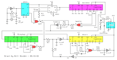
This is a combination digital clock timer and solar panel charge controller used to maintain a deep cycle battery from a solar panel. The timer output is used to control a 12 volt load for a 32 minute time interval each day. Start time is set using 9 dip switches and ends 32 minutes later. The 32 minute duration is set by selecting the 5th bit (2^5 = 32) of a 4040 binary counter (pin 2). The timer also has a manual toggle switch so the load can be manually switched on or off and automatically shuts off after 32 minutes. The time duration can be longer or shorter (8,16,32,64,128,256 minutes etc.) by selecting the appropriate bit of the counter. The timer circuit is shown in the lower schematic just above the regulator.


Digital-Clock-Circuit-Diagram
Basic Clock Circuit Diagram

The basic clock circuit (top schematic below) is similar to the binary clock (on another page) and uses 7 ICs to produce the 20 digital bits for 12 hour time, plus AM and PM. A standard watch crystal oscillator (32,768) is used as the time base and is divided down to 1/2 half second by the 4020 binary counter. One half of a 4013 data latch is used to divide the 1/2 second signal by 2 and produce a one second pulse that drives the seconds counter (74HC390 colored purple). The minutes are advanced by decoding 60 seconds (40 + 20) and then resetting the seconds counter to 0 and at the same time advancing the minutes counter. The same procedure is used to advance the hours. The second half of the 4013 latch is used to indicate AM or PM and is toggled by decoding 13 hours and resetting the hours to 0 and then advancing the hours to "one".

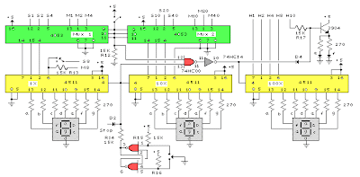
Digital-Clock-Circuit-Diagram-1
Clock Display Circuit Diagram

The clock display circuit is shown in the second drawing below and uses 6 more ICs to decode the binary data and drive four seven segment LED displays. The 10s of hours digit is driven with a single 3904 transistor. Two multiplexer circuits (4053) are used to manually select either minutes or seconds for the right two display digits. The two switches shown between the 4053s and below the left 4053 are both part of one DPDT switch which selects either seconds or minutes for the 1X and 10X digits. This switch is shown in the seconds position and the hours digits are blanked with a low signal on pin 4 of the 4511.

The display can also be toggled on and off (totally blank) using a set/reset latch made from a couple 74HC00 NAND gates. A momentary DPDT switch is used to control the latch and toggle the display on or off. The second pole of this switch is used on the upper drawing (connected to the run/stop switch) to set the hours and minutes. Thus this same switch performs both functions of blanking the display and setting the time. The run/stop switch is shown in the normal running mode and supplies a low signal to a NAND gate which prevents accidental setting the time while the clock is running.

Digital-Clock-Circuit-Diagram-2
Clock Timer Circuit Diagram

The run/stop switch also turns on the display (through the diode D2) when in the stop position. The procedure for setting the clock would be to set the (run/stop) switch the stop position and the (seconds/minutes) switch to the minutes position. Then toggle the momentary switch to set minutes and hours of the current time plus one minute. The clock can then be started with the run/stop switch at precisely the right time (+/- 0.5 seconds).

Digital-Clock-Circuit-Diagram-3
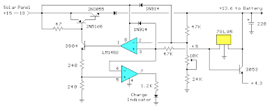
Voltage Regulator (13.6 volts)

The voltage regulator in the lower drawing maintains the battery at 13.6 volts and also supplies the clock and timer circuits with 4.3 volts. The charge LED indicator only comes on when the regulator is supplying max charge to the battery. When the battery voltage reaches 13.6 the regulator reduces the current to whatever is necessary to maintain the voltage and the charge indicator will turn off. The unit I built also included a battery condition indicator (voltmeter using 4 LEDs) to indicate the battery condition so that a failure of the regulator would be indicated by the charge indicator LED turned off and less than 4 LEDs lit on the voltmeter.
Continue[...]